PHYSICAL DESIGN AND DEBUGGING
Power and ground lines have inherent inductance and capacitance, which affect the total impedance of the entire system. Higher impedances reduce current and therefore offer reduced power consumption, while low impedances (ground planes) help minimize prob- lems like noise and cross talk. Hence, it is very important for a designer to have a controlled impedance design where high speed signals are involved. The formula for impedance is as follows:
'Impedance= (ljC)1/2.
The total characteristic impedance for the power supply can be reduced by adding more lines. For
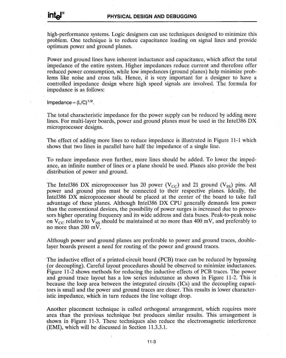
The effect of adding more lines to reduce impedance is illustrated in Figure
To reduce impedance even further, more lines should be added. To lower the imped- ance, an infinite number of lines or a plane should be used. Planes also provide the best distribution of power and ground.
The Intel386 DX microprocessor has 20 power (Ved and 21 ground (Vss) pins. All power and ground pins must be connected to their respective planes. IdealJy, the Inte1386 DX microprocessor should be placed at the center of the board to take full advantage of these planes. Although Inte1386 DX CPU generally demands less power than the conventional devices, the possibility of power surges is increased due to proces- sors higher operating frequency and its wide address and data buses.
Although power and ground planes are preferable to power and ground traces, double- layer boards present a need for routing of the power and ground traces.
'The inductive effect of a
Another placement technique is called orthogonal arrangement, which requires more area than the previous technique but produces similar results. This arrangement is shown in Figure
(EMI), which will be discussed in Section 11.3.3.1. | ' |
|