.
4Kx4
ADDRESS
CACHE SRAM
BANK A (4Kx4)
;
CACHE SUBSYSTEMS
2x373 | A I | 01 | |
_ 0 0 | |||
| |||
| ~2JA13 | I | |
OED E | - | ||
~t |
| ||
- |
| ||
4x245 |
|
| |
| I " |
DATA
CSO#-~
CS3# WEN
4
4
CSO#- OED WEN CS3#
ADDRESS ;L -
CACHE SRAM 'I BANK B
(4K x 32)
A
DATA
'\I
A B |
|
|
|
|
" OED DIR | 'I DO~D31 | ;! | Ul |
|
|
| « | Ul |
|
|
| c | w |
|
|
|
| II: | 82385 |
|
| Ul | c | |
|
| :l | COEA# | CACHE |
74A~~ | ||||
| ~~;CWEA# | CONTROL | ||
|
| 0 | m |
|
|
| 0 |
|
|
|
|
| ||
|
|
| 9 |
|
74AS~~ x~- ~ CWEB# |
| |||
| ~- | COEB# |
| |
|
| ~ | ~~: |
|
OED DIR
" A B | I " | |
|
| |
" | '\I | IV |
~ | ||
|
| ... ;, "'v;' |
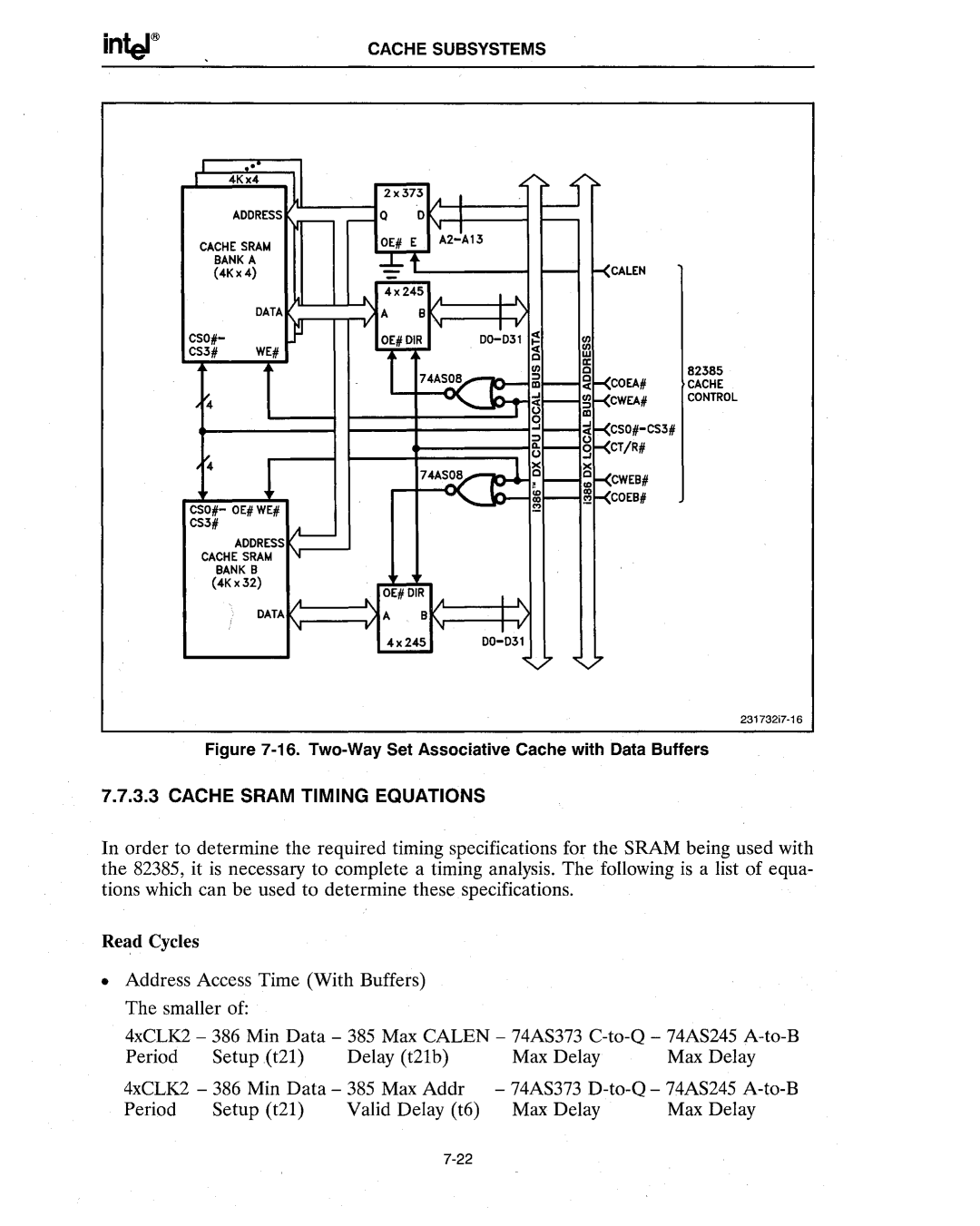
Figure 7-16. Two-Way Set Associative Cache with Data Buffers
7.7.3.3 CACHE SRAM TIMING EQUATIONS
In order to determine the required timing specifications for the SRAM being used with the 82385, it is necessary to complete a timing analysis. The following is a list of equa- tions which can be used to determine these specifications.
Read Cycles
•Address Access Time (With Buffers) The smaller of:
4xCLK2 - 386 Min Data - 385 | Max CALEN - 74AS373 | ||||
Period | Setup (t21) | Delay (t21b) | Max Delay | Max Delay | |
4xCLK2 - 386 Min Data - 385 | Max Addr | - 74AS373 | |||
Period | Setup (t21) | Valid Delay (t6) | Max Delay | Max Delay | |
|
|
|
|
| |