PHYSICAL DESIGN AND DEBUGGING
GNO
Ie Packages
5v
\ . I
~ I Oecoupling
GN0L---T-__+-
1 U·'~"
231732i11-2
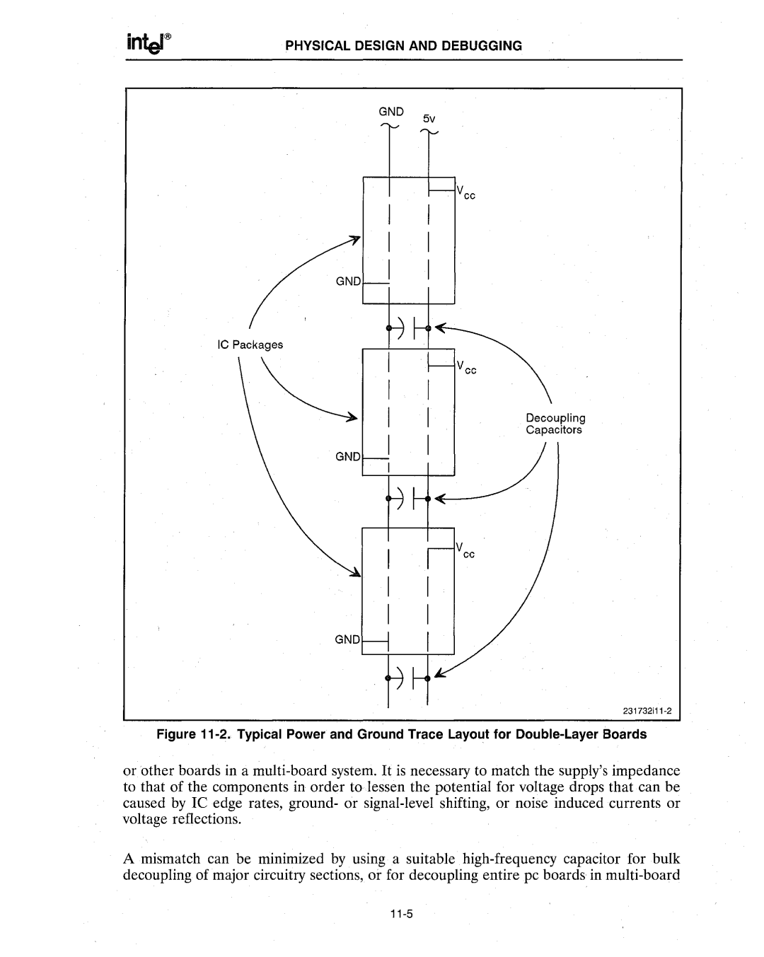
Figure 11-2. Typical Power and Ground Trace Layout for Double-Layer Boards
or other boards in a
A mismatch can be minimized by using a suitable