MULTIBUS I AND Intel386 DX MICROPROCESSOR
•Some slave interrupt controllers reside on local buses, and other slave interrupt con- trollers reside on MULTIBUS I. In this case, the appropriate bus for the interrupt- acknowledge cycle depends on the cascade address generated by the master interrupt controller.
In the first two configurations, no decoding is needed because all interrupt acknowledge cycles are directed to one bus. However, if a system contains a master interrupt control- ler residing on a local bus and at least one slave interrupt controller residing on MUL- TIBUS I, address decoding must select the bus for each interrupt-acknowledge cycle.
The interrupt-acknowledge cycle must be considered in the design of this decoding logic. The Intel386 DX microprocessor responds to an active INTR input by performing two bus cycles. During the first cycle, the master interrupt controller determines which, if any, of its slave controllers should return the interrupt vector and drive sits cascade address pins (CASO#, CASI#, CAS2#) to select that slave controller. During the sec- ond cycle, the Inte1386 DX microprocessor reads an 8-bit vector from the selected inter- rupt controller and uses this vector to service the interrupt.
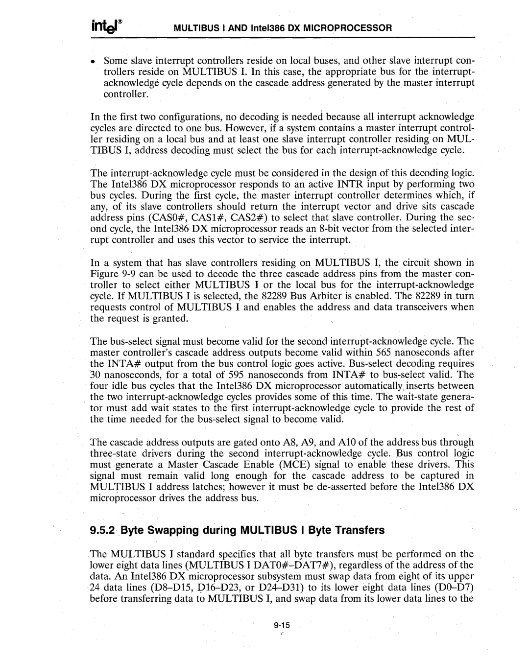
In a system that has slave controllers residing on MULTIBUS I, the circuit shown in Figure 9-9 can be used to decode the three cascade address pins from the master con- troller to select either MULTIBUS I or the local bus for the interrupt-acknowledge cycle. If MULTIBUS I is selected, the 82289 Bus Arbiter is enabled. The 82289 in turn requests control of MULTIBUS I and enables the address and data transceivers when the request is granted.
The bus-select signal must become valid for the second interrupt-acknowledge cycle. The master controller's cascade address outputs become valid within 565 nanoseconds after the INTA# output from the bus control logic goes active. Bus-select decoding requires 30 nanoseconds, for a total of 595 nanoseconds from INTA# to bus-select valid. The four idle bus cycles that the Inte1386 DX microprocessor automatically inserts between the two interrupt-acknowledge cycles provides some of this time. The wait-state genera- tor must add wait states to the first interrupt-acknowledge cycle to provide the rest of the time needed for the bus-select signal to become valid.
The cascade address outputs are gated onto A8, A9, and AIO of the address bus through three-state drivers during the second interrupt-acknowledge cycle. Bus control logic must generate a Master Cascade Enable (MCE) signal to enable these drivers. This signal must remain valid long enough for the cascade address to be captured in MULTIBUS I address latches; however it must be de-asserted before the Intel386 DX microprocessor drives the address bus.
9.5.2Byte Swapping during MULTIBUS I Byte Transfers
The MULTIBUS I standard specifies that all byte transfers must be performed on the lower eight data lines (MULTIBUS I DATO#-DAT7#), regardless of the address of the data. An Intel386 DX microprocessor subsystem must swap data from eight of its upper
24data lines (D8-DI5, DI6-D23, or D24-D31) to its lower eight data lines (DO-D7) before transferring data to MULTIBUS I, and swap data from its lower data lines to the
9-15