APPENDIX B
DRAM PLD DESCRIPTIONS
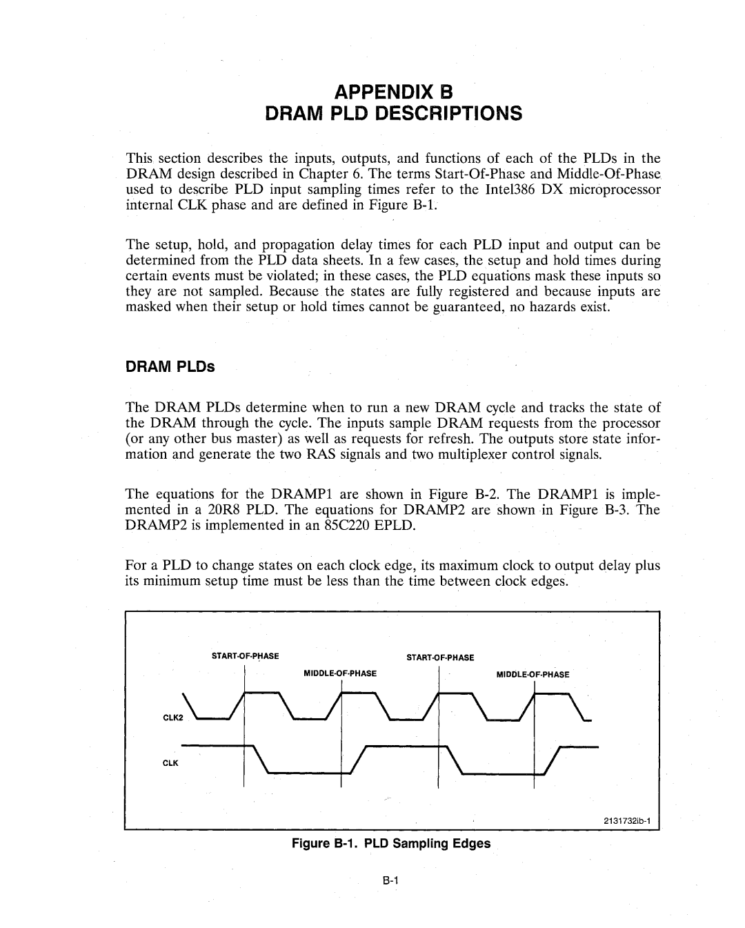
This section describes the inputs, outputs, and functions of each of the PLDs in the DRAM design described in Chapter 6. The terms
The setup, hold, and propagation delay times for each PLD input and output can be determined from the PLD data sheets. In a few cases, the setup and hold times during certain events must be violated; in these cases, the PLD equations mask these inputs so they are not sampled. Because the states are fully registered and because inputs are masked when their setup or hold times cannot be guaranteed, no hazards exist.
DRAM PLDs
The DRAM PLDs determine when to run a new DRAM cycle and tracks the state of the DRAM through the cycle. The inputs sample DRAM requests from the processor (or any other bus master) as well as requests for refresh. The outputs store state infor- mation and generate the two RAS signals and two multiplexer control signals.
The equations for the DRAMPI are shown in Figure
For a PLD to change states on each clock edge, its maximum clock to output delay plus its minimum setup time must be less than the time between clock edges.
START·OF·PHASESTART·OF·PHASE
MIDDLE·OF·PHASEMIDDLE·OF·PHASE