|
|
|
| PHYSICAL DESIGN AND DEBUGGING |
| |||
|
|
|
|
|
| ·PAGE | 66,132 | |
|
|
|
|
| EQUATES |
|
| |
00C8 |
|
|
|
| LATCH | EQU | 0C8H |
|
00AA |
|
|
|
| GOOLSIGNAL | EQU | 0AAH |
|
0055 |
|
|
|
| BALSIGNAL | EQU | 055H |
|
|
|
|
|
| CODE TO VERIFY ABILITY TO WRITE | |||
|
|
|
|
| AND | READ RAM CORRECTLY | ||
0000 |
|
|
|
| INITIAL_CODE | ASSUME | CS:INITIAL_CODE | |
|
|
|
| SEGMENT |
|
| ||
F000 |
|
|
|
|
| ORG | 0F000H | |
F000 | BB | 0000 |
| TSLLOOP: | MOV | BX, | 0000H | |
F003 | 8E | DB |
|
|
| MOV | DS, | BX |
F005 | C7 | 07 | 5473 |
| MOV | [BX1, 5473H | ||
F009 | C7 | 47 | 02 | 2961 |
| MOV | [BX1+2, 2961H | |
F00E | EB | 01 | 90 |
|
| JMP | READ |
|
F011 | 81 | 3F | 5473 | READ: | CMP | [BXl, 5473H | ||
F015 | 75 | 0D |
|
|
| JNE | BADRAM | |
F017 | 81 | 7F | 02 | 2961 |
| CMP | [BX1+2, 2961H | |
F01C | 75 | 06 |
|
|
| JNE | BAD RAM | |
F01E | B0 | AA |
|
|
| MOV | AL, | GOOLSIGNAL |
F020 | E6 | C8 |
|
|
| OUT | LATCH, AL | |
F022 | EB | DC |
|
|
| JMP | TSLLOOP | |
F024 | B0 | 55 |
|
| BADRAM: | MOV | AL, | BALSIGNAL |
F026 | E6 | C8 |
|
|
| OUT | LATCH, AL | |
F028 | EB | D6 |
|
|
| JMP | TSLLOOP | |
FFF0 |
|
|
|
|
| ORG | 0FFF0H | |
FFF0 | E9 | F000 | R | START: | JMP | TSLLOOP | ||
FFF3 |
|
|
|
| INITIAL_CODE | ENDS |
|
|
|
|
|
|
|
| END |
|
|
Warning | Severe |
|
|
|
|
| ||
Errors |
| Errors |
|
|
|
|
| |
0 |
| 0 |
|
|
|
|
|
|
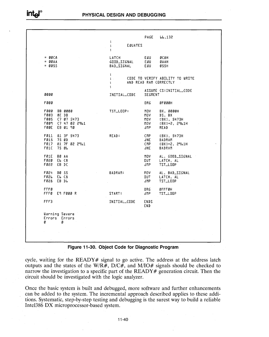
Figure 11-30. Object Code for Diagnostic Program
cycle, waiting for the READY# signal to go active. The address at the address latch outputs and the states of the W/R#, D/C#, and M/IO# signals should be checked to narrow the investigation to a specific part of the READY# generation circuit. Then the circuit should be investigated with the logic analyzer.
Once the basic system is built and debugged, more software and further enhancements can be added to the system. The incremental approach described applies to these addi- tions. Systematic,
