MCF5282 ColdFire Microcontroller User’s Manual
HOW to Reach US USA/EUROPE/LOCATIONS not Listed
IND
IND
Contents
Chapter Enhanced Multiply-Accumulate Unit Emac
Timing Assumptions Move Instruction Execution Times
Chapter Cache
Chapter Static RAM Sram
ColdFire Flash Module CFM
Chapter Power Management
Chapter System Control Module SCM
Clock Module
Interrupt Controller Modules
Signal Descriptions
Chapter Edge Port Module Eport
Chapter Chip Select Module
Chapter External Interface Module EIM
Chapter Synchronous Dram Controller Module
Chapter DMA Controller Module
Chapter Fast Ethernet Controller FEC
Chapter Watchdog Timer Module
Chapter Programmable Interrupt Timer Modules PIT0-PIT3
Chapter General Purpose Timer Modules Gpta and Gptb
20.3
Chapter DMA Timers DTIM0-DTIM3
Chapter Queued Serial Peripheral Interface Qspi Module
Chapter Uart Modules
Chapter I2C Interface
Chapter FlexCAN
Chapter General Purpose I/O Module
Chapter Queued Analog-to-Digital Converter Qadc
27.4.7
Reset Controller Module
Chapter Debug Support
Chapter Chip Configuration Module CCM
Chapter Ieee 1149.1 Test Access Port Jtag
Electrical Characteristics
Chapter Mechanical Data
Appendix a Register Memory Map
Paragraph Title Number 31.6.2 Nonscan Chain Operation 31-12
Illustrations
Title Number
10-7
13-4
17-13
20-20
23-10
25-31
Qadc Status Register 0 QASR0 27-22 27-12
27-53
29-39WDMREG BDM Command Format 29-36 29-40
Tables
Charge Pump Current and MFD in Normal Mode Operation
10-13
15-18
17-30
20-23
25-21
27-13
29-43
33-21 Timer Module AC Timing Specifications 33-24 33-22
Audience
Organization
Organization
Xlv
Suggested Reading
General Information
ColdFire Documentation
Conventions
Acronyms and Abbreviations
Table i. Acronyms and Abbreviated Terms
Meaning
Terminology Conventions
Table ii. Notational Conventions
Operand Syntax
Opcode Wildcard
ACC
CCR
Port Name
PST
LSW
MSW
Revision History
Table iii provides a revision history for this document
Table iii. Revision History
SST
Revision Date Substantive Changes
Number Release
Frsr
Liv
10.3.6/10-11
RAMBAR.’
Revision Number
Substantive Changes Section/Page
MCF5282 Key Features
Chapter Overview
MCF5282 Key Features
MCF5282 Key Features
MCF5282 Key Features
MCF5282 Key Features
MCF5282 Key Features
MCF5282 Block Diagram
Cache Configuration
Configuration Tag Address Data Array Address
Version 2 ColdFire Core
Cache
Sram
Flash
Debug Module
System Control Module
External Interface Module EIM
Power Management
Chip Select
General Input/Output Ports
Interrupt Controllers INTC0/INTC1
Test Access Port
Uart Modules
DMA Timers DTIM0-DTIM3
General-Purpose Timers GPTA/GPTB
Periodic Interrupt Timers PIT0-PIT3
Software Watchdog Timer
Phase Locked Loop PLL
Reset
DMA Controller
MCF5282-Specific Features
MCF5282-Specific Features
Processor Pipelines
IAG
Fifo
Dsoc
Processor Register Description
User Programming Model
Data Registers D0-D7
Address Registers A0-A6
Stack Pointer A7
Program Counter PC
Condition Code Register CCR
Bits Name Description
Emac Programming Model
Supervisor Programming Model
Status Register SR
System Byte Condition Code Register CCR
Bits
Supervisor/User Stack Pointers A7 and OTHERA7
Access Control Registers ACR0, ACR1
Programming Model
Vector Base Register VBR
Cache Control Register Cacr
Additions to the Instruction Set Architecture
Name CPU Space Rc Written with Register Name
Local Memory Registers
Exception Processing Overview
ISA Revision A+ New Instructions
Instruction Description
Exception Vector Assignments
Vector Stacked Program Assignment NumberS Offset Hex Counter
Exception Stack Frame Definition
Format Field Encodings
0x100-0x3FC Next
Access Error Exception
Fault Status Encodings
Processor Exceptions
FS30 Definition
Address Error Exception
Illegal Instruction Exception
Divide-By-Zero
Privilege Violation
Unimplemented Line-A Opcode
Unimplemented Line-F Opcode
Debug Interrupt
RTE and Format Error Exception
Fault-on-Fault Halt
Reset Exception
Trap Instruction Exception
VER REV
MAC DIV Emac FPU MMU ISA Debug
D0 Hardware Configuration Info Field Description
VER
MAC
ICA Icsiz RAM0SIZ ROM0SIZ
Busw DCA Dcsiz RAM1SIZ ROM1SIZ
ICA
4KB RAM
8KB RAM
16KB RAM
32KB RAM
Instruction Execution Timing
Timing Assumptions
Move Instruction Execution Times
10. Misaligned Operand References
Address10 Size Kbus Additional Operations CR/W
11. Move Byte and Word Execution Times
12. Move Long Execution Times
Source Destination Ax+ D16,Ax D8,Ax,Xi Xxx.wl
Standard One Operand Instruction Execution Times
Standard Two Operand Instruction Execution Times
13. One Operand Instruction Execution Times
14. Two Operand Instruction Execution Times
Standard Two Operand Instruction Execution Times
Miscellaneous Instruction Execution Times
15. Miscellaneous Instruction Execution Times
Effective Address Opcode An+ D16,An D8,An,Xn*SF Xxx.wl
D16,PC D8,PC,Xn*SF
Emac Instruction Execution Times
16. Emac Instruction Execution Times
Effective Address Opcode An+ D16,An D8,An,X Xxx.wl #xxx
Branch Instruction Execution Times
ColdFire Instruction Set Architecture Enhancements
17. General Branch Instruction Execution Times
18. BRA, Bcc Instruction Execution Times
Operation
Assembler Syntax
Attributes
Instruction Format
Byte Reverse Register Byterev
Assembler Syntax BYTEREV.L Dx Attributes
Condition Codes
Find First One in Register
Old Dx310 New Dx310
Store/Load Status Register Strldsr
Supported Starting with ISA A+
Assembler SyntaxSTRLDSR #data
Chapter Enhanced Multiply-Accumulate Unit Emac
Multiply-Accumulate Unit
Multiply-Accumulate Functionality Diagram
Introduction to the MAC
General Operation
Infinite Impulse Response IIR Filter
Fractional Alignment
Motorola
Memory Map/Register Set
MAC Status Register Macsr
1describes Macsr fields
Macsr Field Descriptions
Fractional Operation Mode
Rounding
Summary of S/U, F/I, and R/T Control Bits
Operational Modes
Saving and Restoring the Emac Programming Model
Following code performs the Emac state restore
Mask Register Mask
MULS/MULU
MAC.sz Ry,RxSF,eay&,Rw
Command Mnemonic Description
Emac Instruction Set Summary
Emac Instruction Execution Times
3summarizes Emac unit instructions
Data Representation
Mac Mov
Accumulator Mac Old Mov New
MAC Opcodes
Two’s Complement, Signed Fractional Equation
MACSR.V =
Emac Instruction Set Summary
MACSR.Z =
Emac Instruction Set Summary
Motorola
Emac Instruction Set Summary MCF5282 User’s Manual
Cache Features
Cache Physical Organization
This chapter describes the MCF5282 cache operation
Cache Physical Organization
Cache Operation
Interaction with Other Modules
Memory Reference Attributes
Cache Coherency and Invalidation
Cache Miss Fetch Algorithm/Line Fills
Initial Fetch Offset vs. Clnf Bits
CLNF10 Longword Address Bits
Instruction Cache Operation as Defined by CACR31
CACR31 CACR10 Type of Instruction Fetch Description
Cache Programming Model
Cache Registers Memory Map
Cache Registers
Cache Control Register Cacr
Cenb CPD
Cinv Didi Disd Invi Invd
Ceib DCM Dbwe DWP Eusp Clnf
Cenb
Ceib
Cache Configuration as Defined by CACR31, 23
CACR31 CACR23 CACR22 Configuration Description
CACR23 CACR22 CACR21 CACR20 Configuration Operation
Cache Invalidate All as Defined by CACR23, 22, 21
Access Control Registers ACR0, ACR1
External Fetch Size Based on Miss Address and Clnf
Bufw
BWE
Between the processors local bus and the external bus
Sram Features
Sram Operation
Sram Programming Model
Sram Base Address Register Rambar
PRI1 PRI2 SPV
PRI1, PRI2
PRI12 Upper Bank Lower Bank Priority
Sram Initialization
Sram Base Address Register
Power Management
Typical Rambar Setting Examples
Sram Initialization Code
Following loop initializes the entire Sram to zero
Sram Programming Model
Sram Programming Model MCF5282 User’s Manual
Features
Chapter ColdFire Flash Module CFM
Block Diagram
CFM Block Diagram
Memory Map
CFM Array Memory Map
CFM Configuration Field
CFM Configuration Field
Flash Base Address Register Flashbar
Address Offset from array base Size Description
Memory Map
BA30 BA29
CFM Configuration Register Cfmcr
CFM Registers
Register Descriptions
Flash registers are described in this subsection
CFM Clock Divider Register Cfmclkd
Cfmcr Field Descriptions
Bits Name Description
Divld PRDIV8
CFM Security Register Cfmsec
Cfmclkd Field Descriptions
Cfmsec Field Descriptions
SEC150 Description
CFM Protection Register Cfmprot
Cfmprot Field Descriptions
Prot
CFM Supervisor Access Register Cfmsacc
PROTECT31
PROTECT2
Sector
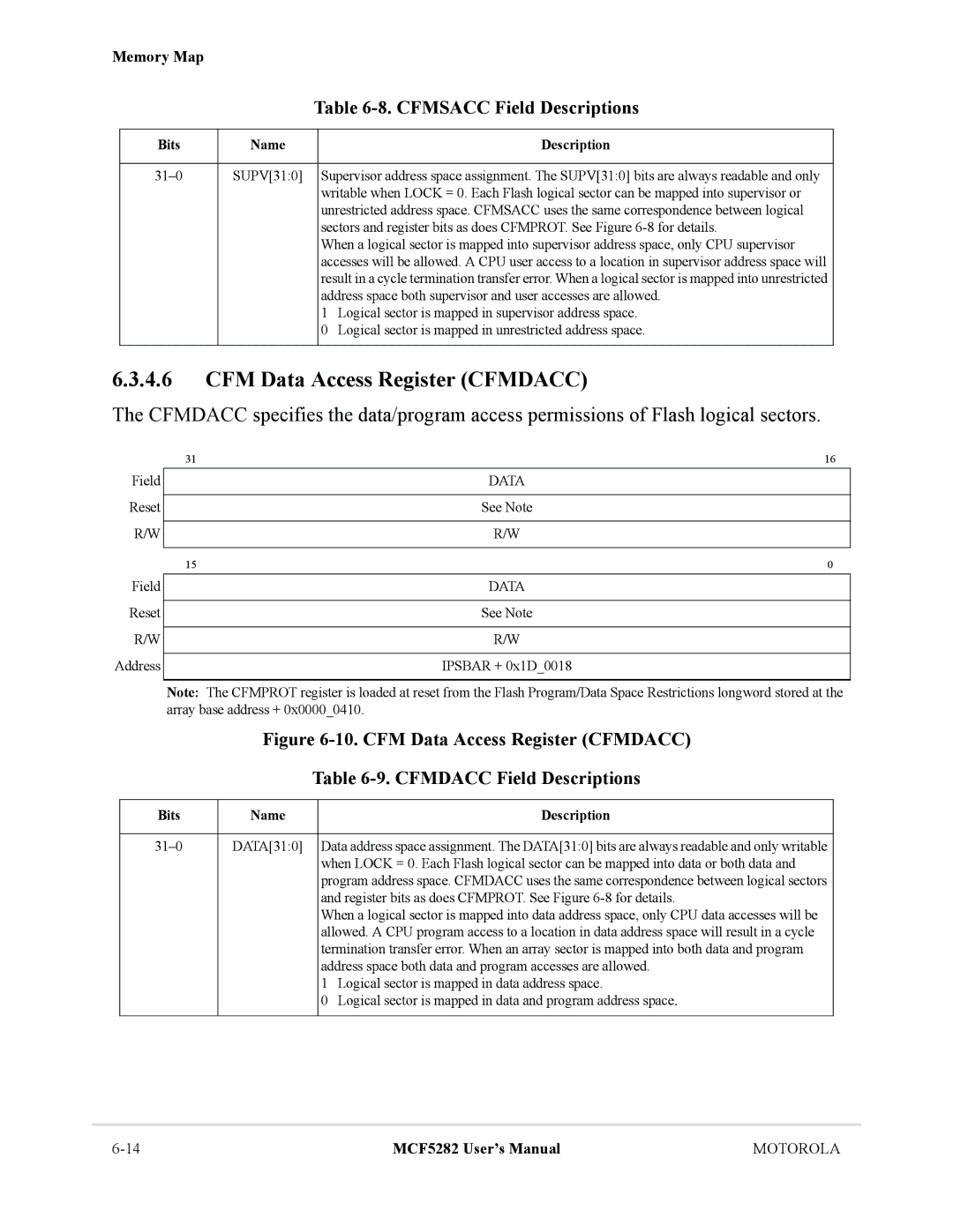
CFM Data Access Register Cfmdacc
Cfmsacc Field Descriptions
Data
CFM User Status Register Cfmustat
Only one Cfmustat bit should be cleared at a time
10. Cfmustat Field Descriptions
Cbeif Ccif Pviol Accerr Blank
CFM Command Register Cfmcmd
12. Cfmcmd User Mode Commands
Command Name Description
CFM Operation
Read Operations
Write Operations
Program and Erase Operations
Setting the Cfmclkd Register
Thus the Flash state machine clock will be
Consider the following example for fSYS = 66 MHz
Program, Erase, and Verify Sequences
Flash Valid Commands
13summarizes the valid Flash user commands
13. Flash User Commands
Meaning Description
13. Example Program Algorithm
Stop Mode
Flash User Mode Illegal Operations
Master Mode
Flash Security Operation
Reset
Back Door Access
Erase Verify Check
Interrupt Source Interrupt Flag Local Enable
Interrupts
14. CFM Interrupt Sources
Cbeif Cbeie
Interrupts MCF5282 User’s Manual
Memory Map and Registers
Programming Model
Low-Power Interrupt Control Register Lpicr
Chip Configuration Module Memory Map
Memory Map
Following subsection describes the PMM registers
Lpicr Field Description
Enbstop
Low-Power Control Register Lpcr
Xlpmipl Settings
Xlpmipl Interrupts Level Needed to Exit Low-Power Mode
Lpmd Stpmd Lvdse
Low-Power Modes
Low-Power Modes
PLL/CLKOUT Stop Mode Operation
Functional Description
Run Mode
Wait Mode
Doze Mode
Stop Mode
Peripheral Behavior in Low-Power Modes
Static Random-Access Memory Sram
Peripheral Shut Down
ColdFire Core
Sdram Controller Sdramc
Chip Select Module
DMA Controller DMAC0-DMA3
Uart Modules UART0, UART1, and UART2
DMA Timers DMAT0-DMAT3
2.9 I2C Module
Queued Serial Peripheral Interface Qspi
Reset Controller
Interrupt Controllers INTC0, INTC1
Fast Ethernet Controller FEC
2.14 I/O Ports
Chip Configuration Module
Clock Module
Watchdog Timer
Programmable Interrupt Timers PIT0, PIT1, PIT2 and PIT3
Edge Port
Queued Analog-to-Digital Converter Qadc
General Purpose Timers Gpta and Gptb
FlexCAN
Functional Description
ColdFire Flash Module
Summary of Peripheral State During Low-Power Modes
CPU and Peripherals in Low-Power Modes
2.25 BDM
Jtag
Qadc
BDM
Jtag
Functional Description MCF5282 User’s Manual
Features
Overview
Memory Map and Register Definition
SCM Register Map
3124 2316 158
Register Descriptions
Internal Peripheral System Base Address Register Ipsbar
Cache
Memory Base Address Register Rambar
Ipsbar Field Description
Memory Base Address Register Rambar Rambar Field Description
BDE
Core Reset Status Register Crsr
Core Watchdog Control Register Cwcr
Crsr Field Descriptions
Register Descriptions
Core Watchdog Timer Delay
CWT CWT Time-Out Period
Core Watchdog Service Register Cwsr
Internal Bus Arbitration
SRAM1 Mpark Rambar CPU DMA EIM
Marb
FEC Sdramc
Round-Robin Mode
Overview
Arbitration Algorithms
Fixed Mode
Fixed Timeout Prklast Lckouttime
Bus Master Park Register Mpark
M2PEN BCR24BIT M3PRTY M2PRTY M0PRTY M1PRTY
Mpark Field Description
System Access Control Unit Sacu
Features
Memory Map/Register Definition
Sacu Register Memory Map
3128 2724 2320 1916 1512 118
PACR1 PACR2 PACR3
Peripheral Access Control Registers Pacr 0-PACR8
Master Privilege Register MPR
PACR6
12. Peripheral Access Control Registers PACRs
Bits Supervisor Mode User Mode
Ipsbar Offset Name Modules Controlled
UART2
Qspi
DTIM0 DTIM1
DTIM2 DTIM3
13. Grouped PeripheralAccess Control Register
14. Gpacr Accessctrl Bit Encodings
Gpacr Field Descriptions
15. Gpacr Address Space
Register Space Protected Modules Protected Ipsbar Offset
GPACR0
EPORT, WDOG, PIT0-PIT3, QADC, GPTA, Gptb
Normal PLL Mode
Modes of Operation
Low-power Mode Operation
2 11 PLL Mode
External Clock Mode
Clock Module Operation in Low-power Modes
Block Diagram
Clock Module Block Diagram
Signal Descriptions
Signal Properties
Extal
Name Function
Memory Map and Registers
Register Descriptions
Synthesizer Control Register Syncr
Lolre MFD2 MFD1 MFD0 Locre
Locen Disclk Fwkup STPMD1 STPMD0
MFD
MFD20
RFD
Synthesizer Status Register Synsr
Stpmd
OSC
Pllmode
Synsr Field Descriptions
Locks
Clock Mode
Functional Description
System Clock Modes
System Clock Modes
Clock Operation During Reset
System Clock Mode PLL Options
System Clock Generation
Clock Out and Clock In Relationships
Phase and Frequency Detector PFD
PLL Operation
Charge Pump Current and MFD in Normal Mode Operation
Charge Pump/Loop Filter
Voltage Control Output VCO
Multiplication Factor Divider MFD
PLL Lock Detection
PLL Loss of Lock Reset
PLL Loss of Lock Conditions
Loss of Clock Reset
Loss of Clock Detection
Alternate Clock Selection
Loss of Clock Summary
Loss of Clock in Stop Mode
10. Stop Mode Operation Sheet 1
10. Stop Mode Operation Sheet 2
Expected PLL Action
Stop
10. Stop Mode Operation Sheet 3
NRM ‘LC ‘LK
‘LC NRM ‘LK
10. Stop Mode Operation Sheet 4
PLL
10. Stop Mode Operation Sheet 5
Lose reference
Clock
Modes
Functional Description MCF5282 User’s Manual
Chapter Interrupt Controller Modules
10.1 68K/ColdFire Interrupt Architecture Overview
68K/ColdFire Interrupt Architecture Overview
Interrupt Controller Theory of Operation
Interrupt Recognition
Interrupt Prioritization
Interrupt Priority Within a Level
Interrupt Vector Determination
Memory Map
Interrupt Controller Base Addresses
Interrupt Controller Memory Map
Interrupt Controller Number Base Address
Interrupt Pending Registers IPRHn, IPRLn
INT
Interrupt Mask Register IMRHn, IMRLn
Intmask
Maskall
Interrupt Force Registers INTFRCHn, INTFRCLn
IMRLn Field Descriptions
Intfrc
Interrupt Request Level Register IRLRn
IRQ
Interrupt Acknowledge Level and Priority Register IACKLPRn
Interrupt Control Register ICRnx, x = 1, 2
11. IACKLPRn Field Descriptions
Level PRI
Interrupt Sources
12. ICRnx Field Descriptions
13. Interrupt Source Assignment for INTC0
IIF
DTIM0 CAP/REF
DTIM1 CAP/REF
DTIM2 CAP/REF
Gptb TOF
PIT0 PIF
PIT1 PIF
PIT2 PIF
Software and Level n Iack Registers SWIACKR, L1IACK-L7IACK
14. Interrupt Source Assignment for INTC1
Prioritization Between Interrupt Controllers
Vector
Low-Power Wakeup Operation
10-18
Low-Power Mode Operation
Introduction
Ipbus
Edge Port Module Operation in Low-power Modes
Low-power Mode Eport Operation Mode Exit
Interrupt/General-Purpose I/O Pin Descriptions
Bits Access
Registers
Edge Port Module Memory Map
Eport Pin Assignment Register Eppar
Eport Data Direction Register Epddr
EPPA7
EPPA5 EPPA4 EPPA3 EPPA2 EPPA1
Edge Port Interrupt Enable Register Epier
Edge Port Data Register Epdr
Epdd Field Descriptions
Edge Port Pin Data Register Eppdr
Edge Port Flag Register Epfr
Epdr Field Descriptions
Epfr Field Descriptions
EPF7-EPF1
11-8
Chip Select Module Signals
1lists signals used by the chip select module
Chip Select Module Signals
Signal Description
Byte Enables/Byte Write Enable Signal Settings
Transfer Size Port Size
D3124 D2316 D158 D70
Chip Select Operation
General Chip Select Operation
External Boot Chip Select Operation
Accesses by Matches in CSARs and DACRs
12.3.1.1 8-, 16-, and 32-Bit Port Sizing
BS2 BS1 BS0
D1918 External Boot Chip Select Configuration
D1918 Boot Device/Data Port Size
Chip Select Registers
Chip Select Registers
Chip Select Module Registers
Chip Select Address Registers CSAR0-CSAR6
CSARs, -2,specify the chip select base addresses
6describes Csarba
Chip Select Mask Registers CSMR0-CSMR6
7describes Csmr fields
CSARn Field Description
Csmr n Field Descriptions
Chip Select Control Registers CSCR0-CSCR6
8describes CSCRn fields
SD,UC
PS1 PS0 BEM Bstr Bstw
CSCRn Field Descriptions
No internal TA is asserted. Cycle is terminated externally
12-10
Bus and Control Signals
ColdFire Bus Signal Summary
Signal Name Description Clkout Edge
Bus Characteristics
Data Transfer Operation
TIP
Chip-Select Module Output Timing Diagram
Bus Cycle Execution
Accesses by Matches in CSCRs and DACRs
Data Transfer Cycle States
Bus Cycle States
State Cycle
Read Cycle
MCF5282
System
Write cycle timing diagram is shown in Figure
Write Cycle
3describes the six states of a basic write cycle
Fast Termination Cycles
Read Cycle with Fast Termination
Back-to-Back Bus Cycles
Burst Cycles
Allowable Line Access Patterns
A32 Longword Accesses
Line Transfers
Line Read Bus Cycles
13shows timing when internal termination is used
Line Write Bus Cycles
16. Line Write Burst 2-1-1-1, Internal/External Termination
Misaligned Operands
17shows a line burst write with one wait-state insertion
19. Example of a Misaligned Longword Transfer 32-Bit Port
13-16
Chapter Signal Descriptions
MCF5282 Block Diagram with Signal Interfaces
MCF5282 Signal Description
Signal Name Abbreviation Function External Memory Interface
Sdram Controller Signals
Signal Name Abbreviation Function
Clock and Reset Signals
Chip Configuration Module
External Interrupt Signals
Queued Serial Peripheral Interface Qspi Signals
FlexCAN Signals
2C Signals
Uart Signals
General Purpose Timer Signals
DMA Timer Signals
Analog-to-Digital Converter Qadc Signals
Debug Support Signals
2lists signals in alphabetical order by abbreviated name
Test Signals
Power and Reference Signals
MCF5282 Alphabetical Signal Index
Abbreviation Function
Vddpll
TCK
MCF5282 Signals and Pin Numbers Sorted by Function
Chip Configuration/Mode Selection
Secondary
External Memory Interface and Ports
Chip Selects
Sdram Controller
External Interrupts Port
Ethernet
FlexCAN
General Purpose Timers
UARTs
DMA Timers
Queued Analog-to-Digital Converter Qadc
Debug and Jtag Test Port Control
Single-Chip Mode
Power Supplies
Test
External Boot Mode
Listing of signals that do not default to a Gpio function
Pin Reset States at Reset Single-Chip Mode
Signal Reset Clock and Reset Signals
14.2 MCF5282 External Signals
External Interface Module EIM Signals
Address Bus A230
Data Bus D310
Output Enable OE
Transfer Error Acknowledge TEA
Transfer Acknowledge TA
Read/Write R/W
Transfer Start TS
Transfer In Progress TIP
Chip Selects CS60
Transfer Size Encoding
Sdram Controller Signals
Clock and Reset Signals
Chip Configuration Signals
External Interrupt Signals
Ethernet Module Signals
Transmit Error Etxer
Collision Ecol
Receive Clock Erxclk
Receive Data Valid Erxdv
Queued Serial Peripheral Interface Qspi Signals
FlexCAN Signals
14.2.9 I2C Signals
Uart Module Signals
General Purpose Timer Signals
DMA Timer Signals
Analog-to-Digital Converter Signals
Debug Support Signals
Breakpoint/Test Mode Select BKPT/TMS
Development Serial Input/Test Data DSI/TDI
Development Serial Output/Test Data DSO/TDO
Test Clock Tclk
Test Signals
Debug Data DDATA30
Processor Status Outputs PST30
Test Test
Power and Reference Signals
14-34
Overview
Definitions
Block Diagram and Major Components
DACR0
DACR1
Scas Sras Scke SDRAMCS10 Dramw
Sdram Commands
Command Definition
Sdram Controller Operation
Dram Controller Signals
2describes the behavior of Dram signals in synchronous mode
Memory Map for Sdramc Registers
Dram controller registers memory map is shown in Table
Dram Control Register DCR
DCR, shown in -2,controls refresh logic
4describes DCR fields
DCR Field Descriptions
Dram Address and Control Registers DACR0/DACR1
5describes DACRn fields
DACRn Field Descriptions
Bit
15-7
Bit Associated Access Type Access Definition
Dram Controller Mask Registers DMR0/DMR1
6describes DMRn fields
DMRn Field Descriptions
General Synchronous Operation Guidelines
Address Multiplexing
Generic Address Multiplexing Scheme
Address Pin Row Address Column Address
Pins Row Column
Pins
MCF5282
Row Column
15-12
Burst Page Mode
Pins MCF5282
Sdram Byte Strobe Connections
Interfacing Example
Burst Read Sdram Access
Burst Write Sdram Access
Auto-Refresh Operation
Self-Refresh Operation
Auto-Refresh Operation
Initialization Sequence
Self-Refresh Operation
Mode Register Settings
25. Sdram Example Specifications
Parameter Specification
Sdram Example
Clkout
Sdram Interface Configuration
DCR Initialization
Dacr Initialization
26. Sdram Hardware Connections
Bits Name Setting Description
DACRs should be programmed as shown in Figure
28. Dacr Initialization Values
Casl CBM Imrs
DMR Initialization
29. DMR0 Initialization Values
Mode Register Initialization
30. Mode Register Initialization
31. Mode Register Mapping to MCF5282 A310
MCF5282 Pins Sdram Pins Mode Register Initialization
Mode Register Initialization Sequence
Initialization Code
Precharge Sequence
Refresh Sequence
15-25
15-26
Chapter DMA Controller Module
DMA Module Features
Channel 0 Channel 1 Channel 2 Channel
DMA Request Control Dmareqc
DMA Transfer Overview
DMA
DMA Controller Module Programming Model
Memory Map for DMA Controller Module Registers
Source Address Registers SAR0-SAR3
Destination Address Registers DAR0-DAR3
SAR
DAR
Byte Count Registers BCR0-BCR3
BCR
DMA Control Registers DCR0-DCR3
3describes DCRn fields
DCRn Field Descriptions
BWC Sinc Ssize Dinc Dsize Start
BWC
Encoding BCR24BIT =
DMA Status Registers DSR0-DSR3
4describes DSRn fields
DSR n Field Descriptions
DMA Controller Module Functional Description
Transfer Requests Cycle-Steal and Continuous Modes
BSY
Done
Data Transfer Modes
Dual-Address Transfers
Channel Initialization and Startup
Channel Prioritization
Programming the DMA Controller Module
Data Transfer
Auto-Alignment
Termination
Bandwidth Control
16-16
Chapter Fast Ethernet Controller FEC
Full and Half Duplex Operation
Interface Options
17.2.2.1 10 Mbps and 100 Mbps MII Interface
Primary operational modes are described in this section
17.2.2.2 10 Mpbs 7-Wire Interface Operation
Address Recognition Options
Internal Loopback
FEC Top-Level Functional Diagram
PAD
17-5
Initialization Sequence
User Initialization Prior to Asserting Ecretheren
Hardware Controlled Initialization
Ecretheren De-Assertion Effect on FEC
Microcontroller Initialization
User Initialization After Asserting Ecretheren
FEC User Initialization Before Ecretheren
Microcontroller Initialization
MII Mode
Wire Mode Configuration
Signal Description Emac pin
Network Interface Options
FEC Frame Transmission
FEC Frame Reception
Ethernet Address Recognition
Ethernet Address Recognition-Receive Block Decisions
Hash Algorithm
Ethernet Address Recognitionq-Microcode Decisions
Destination Address to 6-Bit Hash
Bit DA Bit Hash Hash Decimal Hex Value
17-15
Pause Frame Field Specification
Full Duplex Flow Control
Inter-Packet Gap IPG Time
Collision Handling
Internal and External Loopback
Ethernet Error-Handling Procedure
Transmission Errors
Reception Errors
Heartbeat
Top Level Module Memory Map
Detailed Memory Map Control/Status Registers
Module Memory Map
10. FEC Register Memory Map
MIB Block Counters Memory Map
11. MIB Counters Memory Map
Mnemonic Description Offset
Registers
Ethernet Interrupt Event Register EIR
Following sections describe each register in detail
Hberr Ieeetsqe
Babr Babt GRA TXF TXB RXF RXB MII Eberr
17-25
Interrupt Mask Register Eimr
Receive Descriptor Active Register Rdar
Babr Babt GRA TXF TXB RXF RXB MII
Transmit Descriptor Active Register Tdar
Rdesactive
Etheren Reset
Ethernet Control Register ECR
Xdesactive
MII Management Frame Register Mmfr
16. ECR Field Descriptions
Data
17. Mmfr Field Descriptions
Bit Name Description
MII Speed Control Register Mscr
Dispreamble Miispeed
Dispreamble
Mibdisable Mibidle
Mibdisable
MIB Control Register Mibc
19. Programming Examples for Mscr
Receive Control Register RCR
Maxfl
FCE Bcrej Prom Miimode DRT Loop
FCE
Transmit Control Register TCR
Tfcpause Fden
GTS
Physical Address Low Register Palr
22. TCR Field Descriptions
Tfcpause
Physical Address High Register Paur
PADDR1
PADDR2
Type
Opcode/Pause Duration Register OPD
Descriptor Individual Upper Address Register Iaur
24. Paur Field Descriptions
Opcode
Descriptor Individual Lower Address Ialr
IADDR1
Bits Name Descriptions
IADDR2
Descriptor Group Upper Address Gaur
Descriptor Group Lower Address Galr
27. Ialr Field Descriptions
GADDR1
Fifo Transmit Fifo Watermark Register Tfwr
GADDR2
Xwmrk
Fifo Receive Bound Register Frbr
30. Tfwr Field Descriptions
Rbound
Fifo Receive Start Register Frsr
Receive Descriptor Ring Start Erdsr
Rfstart
Transmit Buffer Descriptor Ring Start Etsdr
Rdesstart
Xdesstart
Receive Buffer Size Register Emrbr
34. Etdsr Field Descriptions
Rbufsize
Buffer Descriptors
Driver/DMA Operation with Buffer Descriptors
Driver/DMA Operation with Transmit BDs
Driver/DMA Operation with Receive BDs
Ethernet Receive Buffer Descriptor RxBD
RO1 RO2
36. Receive Buffer Descriptor Field Definitions
Word Location Field Name Description
RO1
Erdsr
Ethernet Transmit Buffer Descriptor TxBD
TO1 TO2 ABC
TO1
17-51
17-52
Watchdog Module Operation in Low-power Modes
Low-power Mode Watchdog Operation Mode Exit
Signals
Watchdog timer module has no off-chip signals
Refer to -2for an overview of the watchdog memory map
16-bit WCR configures watchdog timer operation
Watchdog Timer Module Memory Map
Watchdog Control Register WCR
Watchdog Modulus Register WMR
WCR Field Descriptions
Watchdog Service Register WSR
Watchdog Count Register Wcntr
WMR Field Descriptions
WC9 WC8
WS9 WS8
WS7 WS6 WS5 WS4 WS3 WS2 WS1 WS0
Chapter Programmable Interrupt Timer Modules PIT0-PIT3
PIT module has no off-chip signals
PIT Module Operation in Low-power Modes
Low-power Mode PIT Operation Mode Exit
Programmable Interrupt Timer Modules Memory Map
Ipsbar Offset Access For PITx Bits Address
PIT Control and Status Register Pcsr
PRE3 PRE2 PRE1 PRE0
Doze Halted OVW PIE PIF RLD
PRE
PIT Modulus Register PMR
PIF
Set-and-Forget Timer Operation
PIT Count Register Pcntr
This subsection describes the PIT functional operation
Free-Running Timer Operation
Timeout Specifications
System clock
PIT Clock Counter
Interrupt Request Flag Enable Bit Timeout
Interrupt Operation
4shows the interrupt request generated by the PIT
PIT Interrupt Requests
Chapter General Purpose Timer Modules Gpta and Gptb
GPT Block Diagram
Signal Description
Function Reset State Pull-up Name Register Bit
GPTn20
Pin
Ipsbar Offset Bits Access
GPTn3
SYNCn
GPT Modules Memory Map
GPT Input Capture/Output Compare Select Register Gptios
IOS
GPT Compare Force Register Gpcforc
GPT Output Compare 3 Mask Register GPTOC3M
Gptios Field Descriptions
FOC
GPT Output Compare 3 Data Register GPTOC3D
GPT Counter Register Gptcnt
GPTOC3M Field Descriptions
OC3D
GPT System Control Register 1 GPTSCR1
Gptcnt Field Descriptions
Gpten Tffca
Gpten
GPT Toggle-On-Overflow Register Gpttov
GPT Control Register 1 GPTCTL1
TOV
OM3 OL3 OM2
GPT Interrupt Enable Register Gptie
GPT Control Register 2 GPTCTL2
11. GPTCL1 Field Descriptions
EDG3B EDG3A EDG2B EDG2A
GPT System Control Register 2 GPTSCR2
13. Gptie Field Descriptions
GPT Flag Register 1 GPTFLG1
GPT Flag Register 2 GPTFLG2
GPT Channel Registers GPTCn
Pulse Accumulator Control Register Gptpactl
Ccnt
PAE Pamod Pedge CLK Paovi PAI
Pulse Accumulator Flag Register Gptpaflg
Paclk
Paovf Paif
Pulse Accumulator Counter Register Gptpacnt
19. Gptpaflg Field Descriptions
Pacnt
GPT Port Data Register Gptport
GPT Port Data Direction Register Gptddr
22. Gptddr Field Descriptions
Portt
Prescaler
Input Capture
Output Compare
Event Counter Mode
Pulse Accumulator
Gated Time Accumulation Mode
General-Purpose I/O Ports
Pulse Accumulator
OM3 OL3
23. GPT Settings and Pin Functions
EDGx OMx OC3Mx Pin Data Driven Comments
Dir Function
Reset
24lists the interrupt requests generated by the timer
Interrupt Request Flag Enable Bit
Interrupts
Timer Overflow TOF
GPT Channel Interrupts CnF
Pulse Accumulator Overflow Paovf
Pulse Accumulator Input Paif
20-23
20-24
Chapter DMA Timers DTIM0-DTIM3
DMA Timer Programming Model
Key Features
Prescaler
Capture Mode
Output Mode
DMA Timer Module Memory Map
Reference Compare
DMA Timer Mode Registers DTMRn
Orri FRR CLK RST
DMA Timer Extended Mode Registers DTXMRn
2describes the DTMRn fields
DTMRn Field Descriptions
DTXMR3
DMA Timer Event Registers DTERn
3describes the DTXMRn fields
DTXMRn Field Descriptions
DMA Timer Reference Registers DTRRn
DMA Timer Capture Registers DTCRn
4describes the DTERn fields
DTERn Field Descriptions
Using the DMA Timer Modules
DMA Timer Counters DTCNn
Code Example
Calculating Time-Out Values
T0LOOP
Chapter Queued Serial Peripheral Interface Qspi Module
Module Description
Interface and Signals
Qspi RAM
Qspiclk
Qspi Input and Output Signals and Functions
Signal Name Hi-Z or Actively Driven Function
Operation
Internal Bus Interface
Qspi RAM
Receive RAM
Relative Address Register 0x00
0x01
0x0F
Command RAM
Baud Rate Selection
Transmit RAM
Transfer Delays
Qspiclk Frequency as Function of System Clock and Baud Rate
System Clock
66.67 MHz
Transfer Length
Programming Model
Qspi Registers
Qspi Mode Register QMR
4gives QMR field descriptions
QMR Field Descriptions
Value Bits per transfer
Qspi Delay Register Qdlyr
Qspics Qmrcpol =
Qmrcpha = = Qdlyrqcd Qcrcont = = Qdlyrdtl
QCD
Qspi Wrap Register QWR
5gives Qdlyr field descriptions
6gives QWR field descriptions
Qdlyr Field Descriptions
Qspi Interrupt Register QIR
7describes QIR fields
QIR Field Descriptions
Qspi Address Register QAR
Qspi Data Register QDR
Addr
Command RAM Registers QCR0-QCR15
8gives QCR field descriptions
QCR0-QCR15 Field Descriptions
Programming Example
QSPICS30
Qspiclk QS2 Qspidout QS3 Qspidin
QS4 QS5
22-17
22-18
Uart
Ucts Urts Urxd Utxd
Serial Module Overview
Register Descriptions
Uart Module Memory Map
Ipsbar Offset 3124 2316 158
Uart Mode Registers 1 UMR1n
ERR
Parity Mode Parity Type PT=
2describes UMR1n fields
UMR1n Field Descriptions
CTS
Uart Mode Register 2 UMR2n
3describes UMR2n fields
UMR2 n Field Descriptions
Uart Status Registers USRn
4describes USRn fields
UMR2n Field Descriptions
USRn Field Descriptions
Uart Clock Select Registers UCSRn
5describes UCSRn fields
RCS TCS
Uart Command Registers UCRn
UCSRn Field Descriptions
RCS
Dtin
Bits Value Command Description
UCR n Field Descriptions
Uart Receive Buffers URBn
Uart Transmit Buffers UTBn
UCRn Field Descriptions
Uart Input Port Change Registers UIPCRn
7describes UIPCRn fields
Uipcr n Field Descriptions
COS CTS
UACRs, shown in -7,control the input enable
Uart Auxiliary Control Register UACRn
Uart Interrupt Status/Mask Registers UISRn/UIMRn
8describes UACRn fields
Uart Baud Rate Generator Registers UBG1n/UBG2n
9describes UISRn and UIMRn fields
Uisr n/UIMR n Field Descriptions
Uart Output Port Command Registers UOP1n/UOP0n
Uart Input Port Register UIPn
10describes UIPn fields
11describes UOP1 and UOP0 fields
11. UOP1/UOP0 Field Descriptions
Uart Module Signal Definitions
IRQ
Ucts
12. Uart Module Signals
Transmitter/Receiver Clock Source
Programmable Divider
Following sections describe how to calculate baud rates
Calculating Baud Rates
System Clock Baud Rates
Sysclk
Transmitter and Receiver Operating Modes
Transmitter
Therefore UBG1n = 0x00 and UBG2n = 0xD6
External Clock
23-21
20. Transmitter Timing Diagram
Receiver
Fifo Stack
21shows receiver functional timing
23-24
Automatic Echo Mode
Local Loop-Back Mode
Looping Modes
Multidrop Mode
Remote Loop-Back Mode
25. Multidrop Mode Timing Diagram
Bus Operation
Programming
Read Cycles
Write Cycles
Setting up the Uart to Generate Core Interrupts
Setting up the Uart to Request DMA Service
Interrupt and DMA Request Initialization
13. Uart Interrupts
Register Setting
Uart Module Initialization Sequence
15shows the Uart module initialization sequence
14. Uart DMA Requests
26. Uart Mode Programming Flowchart Sheet 1
26. Uart Mode Programming Flowchart Sheet 2
26. Uart Mode Programming Flowchart Sheet 3
26. Uart Mode Programming Flowchart Sheet 4
26. Uart Mode Programming Flowchart Sheet 5
23-36
Interface Features
Chapter I2C Interface
Acknowledge bit generation/detection Bus-busy detection
Ifdr
Iadr
SCL SDA
24.3 I2C System Configuration
24.4 I2C Protocol
Arbitration Procedure
Repeated Start
Clock Synchronization
Handshaking
Clock Stretching
SCL1 SCL2
24.5.1 I2C Address Register I2ADR
2describes I2ADR fields
I2C Interface Memory Map
I2ADR Field Descriptions
24.5.2 I2C Frequency Divider Register I2FDR
3describes I2FDRIC
I2FDR Field Descriptions
Divider
24.5.3 I2C Control Register I2CR
4describes I2CR fields
I2CR Field Descriptions
IEN Iien
24.5.4 I2C Status Register I2SR
5describes I2SR fields
I2SR Field Descriptions
ICF Iaas IBB IAL SRW IIF
24.6 I2C Programming Examples
24.5.5 I2C Data I/O Register I2DR
Generation of Start
Post-Transfer Software Response
24.6.4 Generation of Stop
I2SR
Slave Mode
Generation of Repeated Start
Arbitration Lost
RXAK=
IAAS=1
SRW=1
Write
24-16
Chapter FlexCAN
RAM MB3 MB2 MB1 MB0
Cantx Canrx
25.1.2 External Signals
FlexCAN Memory Map
FlexCAN Memory Map
Can System
Message Buffers
Message Buffer Structure
Typical can system is shown below in Figure
Common Fields for Extended and Standard Format Frames
Common Extended/Standard Format Frames
Message Buffer Codes for Receive Buffers
Message Buffer Codes for Transmit Buffers
Message Buffer Memory Map
Fields for Extended Format Frames
Fields for Standard Format Frames
Extended Format Frames
Functional Overview
Message Buffers
Idhigh Idlow
Transmit Process
Receive Process
Message Buffer Handling
Self-Received Frames
Serial Message Buffers SMBs
Transmit Message Buffer Deactivation
Receive Message Buffer Deactivation
Remote Frames
Locking and Releasing Message Buffers
Listen-Only Mode
Overload Frames
Time Stamp
Configuring the FlexCAN Bit Timing
Bit Timing
Examples of System Clock/CAN Bit-Rate/S-Clock
Freq Mhz Time-quanta/bit Value +
FlexCAN Error Counters
FlexCAN Initialization Sequence
Debug Mode
Low-Power Stop Mode for Power Saving
Special Operating Modes
Canmcr
Auto-Power Save Mode
Interrupts
Can Module Configuration Register Canmcr
Programmer’s Model
8describes the Canmcr fields
Stop FRZ Halt Notrdy Wakemsk Softrst Frzack
Canmcr Field Descriptions
Stop
FlexCAN Control Register 0 CANCTRL0
9describes the CANCTRL0 fields
10. Transmit Pin Configuration
Transmit Pin Configuration
FlexCAN Control Register 1 CANCTRL1
11describes the CANCTRL1 fields
Prescaler Divide Register Presdiv
12describes the Presdiv fields
11. CANCTRL1 Field Descriptions
Samp
FlexCAN Control Register 2 CANCTRL2
13describes the CANCTRL2 fields
12. Presdiv Field Descriptions
13. CANCTRL2 Field Descriptions
Free Running Timer Timer
14describes the Timer fields
14. Timer Field Descriptions
Rx Mask Registers
Receive Mask Registers RXGMASK, RX14MASK, RX15MASK
12. Rx Mask Registers RXGMASK, RX14MASK, and RX15MASK
FlexCAN Error and Status Register Estat
17describes the Estat fields
16. RXGMASK, RX14MASK, and RX15MASK Field Descriptions
17. Estat Field Descriptions
Biterr
Interrupt Mask Register Imask
18describes the Imask fields
BUF15M BUF14M BUF13M
BUF10M BUF9M BUF8M
Interrupt Flag Register Iflag
19describes the Iflag fields
18. Imask Field Descriptions
19. Iflag Field Descriptions
FlexCAN Receive Error Counter Rxectr
FlexCAN Transmit Error Counter Txectr
20describes the Rxectr fields
21describes the Txectr fields
Chapter General Purpose I/O Module
MCF5282 Ports Module Block Diagram
Features
Sdram control Bit DMA timers Uart transmit/receive
Overview
Modes of Operation
External Signal Description
MCF5282 Ports External Signals
Erxer
SDA
SCL
UCTS0
31-24 23-16 15-8 Access
Memory Map/Register Definition
Register Overview
MCF5282 Ports Module Memory Map
Ddrb Ddrc
Ddreh Ddrel
Clra Clrb Clrc Clrd
Clre Clrf Clrg Clrh
Port Output Data Registers PORTn
Port Output Data Registers 8-bit
Port Data Direction Registers DDRn
PORTn bits are described in Table
PORTn 8-bit, 7-bit, 6-bit, and 4-bit Field Descriptions
Register Bits Name Description
Port Data Direction Register 7-bit
Port Pin Data/Set Data Registers PORTnP/SETn
10. Port Pin Data/Set Data Registers 8-bit
Port Clear Output Data Registers CLRn
PORTnP/SETn bits are described in Table
PORTnP/SETn 8-bit, 6-bit, and 4-bit Field Descriptions
PORTUAP/SETUA
CLRn register bits are described in Table
CLRn 8-bit,7-bit, 6-bit, and 4-bit Field Descriptions
Reset Values for Pbcdpar Bits
Port Size Pbpa Reset Pcdpa Reset
External Boot
Port B/C/D Pin Assignment Register Pbcdpar
Port E Pin Assignment Register Pepar
Pepar Field Descriptions
PEPA3
10. Reset Values for Pepar Bits and Fields
Single chip mode
Port F Pin Assignment Register Pfpar
Pfpar controls the pin function of port F75
11. Pfpar Field Descriptions
Port J Pin Assignment Register Pjpar
Pjpar controls the pin function of port J
12. Pjpar Field Descriptions
Port SD Pin Assignment Register Psdpar
Port AS Pin Assignment Register Paspar
Psdpar controls the pin function of port SD
Paspar controls the pin function of port AS
Port EH/EL Pin Assignment Register Pehlpar
14. Paspar Field Descriptions
Port QS Pin Assignment Register Pqspar
Pqspar controls the pin function of port QS
15. Pehlpar Field Descriptions
ECOL, ERXCLK, ERXDV, ERXD0, Ecrs
Port TC Pin Assignment Register Ptcpar
Ptcpar controls the pin function of port TC
PTCPA3 PTCPA2 PTCPA1 PTCPA0
Port TD Pin Assignment Register Ptdpar
Ptdpar controls the pin function of port TD
PTDPA3 PTDPA2 PTDPA1 PTDPA0
Port UA Pin Assignment Register Puapar
Puapar controls the pin function of port UA
Port Digital I/O Timing
Clkout Input PIN Register PIN Data
Initialization/Application Information
Clkout Output Data Register Output PIN
Chapter Queued Analog-to-Digital Converter Qadc
Qadc Block Diagram
Debug Mode
Modes of Operation
Port QA Signal Functions
Port QA Analog Input Signals
Port QB Signal Functions
Port QA Digital Input/Output Signals
Port QB Analog Input Signals
External Trigger Input Signals
Multiplexed Address Output Signals
Multiplexed Analog Input Signals
Port QB Digital I/O Signals
Voltage Reference Signals
Dedicated Analog Supply Signals
Dedicated Digital I/O Port Supply Signal
Multiplexed Analog Input Channels
Qadc Module Configuration Register Qadcmcr
This subsection describes the Qadc registers
Qadc Memory Map
Qadc Test Register Qadctest
Port Data Registers Portqa and Portqb
Port QA and QB Data Direction Register Ddrqa and Ddrqb
ANZ ANY ANX ANW
Control Registers
Qadc Control Register 0 QACR0
This subsection describes the Qadc control registers
Qadc Control Register 0 QACR0 QACR0 Field Descriptions
QPR6
Prescaler fSYS Divide-by Values
QPR60
Divisor
Qadc Control Register 1 QACR1
CIE1 PIE1 SSE1
CIE1
Operating Mode
Queue 1 Operating Modes
Qadc Control Register 2 QACR2
CIE2 PIE2 SSE2
Resume
QACR2 Field Descriptions
Queue 2 Operating Modes
CIE2
BQ2
Status Registers
Qadc Status Register 0 QASR0
This subsection describes the Qadc status registers
MQ2128 Operating Modes
27-20
Queued Analog-to-Digital Converter Qadc 27-21
CF1 PF1 CF2
QS9 QS8
QS7 QS6 CWP5 CWP4 CWP3 CWP2 CWP1 CWP0
Scan Mode Queue Operation PF Asserts?
10. QASR0 Field Descriptions
11. CCW Pause Bit Response
CWP
12. Queue Status
Queue 1/Queue 2 States
12. Queue Status Transition
Conversion Command Word Table CCW
Qadc Status Register 1 QASR1
BYP
IST1 IST0
Non-Multiplexed Input Signals Channel Number
Port Signal Name
15. Input Sample Times
IST10 Input Sample Times
17. Multiplexed Channel Assignments and Signal Designations
Multiplexed Input Signals Channel Number
Result Registers
Right-Justified Unsigned Result Register Rjurr
Left-Justified Signed Result Register Ljsrr
Left-Justified Unsigned Result Register Ljurr
18. Rjurr Field Descriptions
Result
27.7 Functional Description
Result Coherency
External Multiplexing
External Multiplexing Operation
18. External Multiplexing Configuration
Analog Subsystem
Module Version Options
Analog-to-Digital Converter Operation
21. Analog Input Channels
19. Qadc Analog Subsystem Block Diagram
Conversion Cycle Times
Channel Decode and Multiplexer
Sample Buffer
Digital Control Subsystem
Comparator
Bias
Successive Approximation Register SAR
Queue Priority Timing Examples
Queue Priority
22. Qadc Queue Operation with Pause
Queue Priority Schemes
22. Trigger Events
23. Status Bits
Events
23. CCW Priority Situation
24. CCW Priority Situation
26. CCW Priority Situation
28. CCW Priority Situation
30. CCW Priority Situation
32. CCW Priority Situation
34. CCW Freeze Situation
38. CCW Freeze Situation
Boundary Conditions
Disabled Mode
Reserved Mode
Scan Modes
Single-Scan Modes
Software-Initiated Single-Scan Mode
Externally Triggered Single-Scan Mode
Externally Gated Single-Scan Mode
Interval Timer Single-Scan Mode
Continuous-Scan Modes
Software-Initiated Continuous-Scan Mode
Externally Triggered Continuous-Scan Mode
Externally Gated Continuous-Scan Mode
Periodic Timer Continuous-Scan Mode
Qadc Clock Qclk Generation
Periodic/Interval Timer
42. Qadc Clock Subsystem Functions
Conversion Command Word Table
43illustrates the operation of the queue structure
43. Qadc Conversion Queue Operation
Queued Analog-to-Digital Converter Qadc 27-61
Signal Connection Considerations
Result Word Table
Analog Reference Signals
Analog Power Signals
45. Errors Resulting from Clipping
Conversion Timing Schemes
46. External Positive Edge Trigger Mode Timing with Pause
47. Gated Mode, Single Scan Timing
Analog Supply Filtering and Grounding
48. Gated Mode, Continuous Scan Timing
49. Star-Ground at the Point of Power Supply Origin
50. Input Signal Subjected to Negative Stress
Accommodating Positive/Negative Stress Conditions
Iinjn
Iinjp
Analog Input Considerations
52. External Multiplexing of Analog Signal Sources
Analog Input Pins
53. Electrical Model of an A/D Input Signal
Settling Time for the External Circuit
24. External Circuit Settling Time to 1/2 LSB
Source Resistance RF + Rsrc 100 Ω 10 kΩ 100 kΩ
Error Resulting from Leakage
25. Error Resulting from Input Leakage IOff
Interrupt Operation
Interrupt Sources
26. Qadc Status Flags and Interrupt Sources
Queue Queue Activity Status Interrupt Flag
PF1 PIE1
Chapter Reset Controller Module
Reset Controller Signal Properties
Rsti
Rsto
Name Direction Input
Reset Control Register RCR
Reset Controller Memory Map
Reset Status Register RSR
Lvdf
Lvdie
Soft WDR POR
RSR Field Descriptions
WDR
Reset Sources
Power-On Reset
Reset Source Summary
Source Type
External Reset
Watchdog Timer Reset
Loss-of-Clock Reset
Loss-of-Lock Reset
Reset Control Flow
Reset Control Flow
Concurrent Resets
Synchronous Reset Requests
Internal Reset Request
Power-On Reset/Low-Voltage Detect Reset
Reset Status Flags
28-12
Debug module is shown in Figure
Processor/Debug Module Interface
Signal Description
Debug Module Signals
Real-Time Trace Support
Processor Status Encoding
PST30 Definition Hex
Begin Execution of Taken Branch PST =
PST30 Definition Hex Binary
Clkout PST
Ddata
Aatr
Ablr
Abhr
CSR
Revision a Shared Debug Resources
BDM/Breakpoint Registers
Rev. a Shared BDM/Breakpoint Hardware
DRc4-0 Register Name Abbreviation Initial State
Address Attribute Trigger Register Aatr
5describes Aatr fields
Aatr Field Descriptions
TMM
Address Breakpoint Registers ABLR, Abhr
Address Breakpoint Registers ABLR, Abhr
Configuration/Status Register CSR
6describes Ablr fields
7describes Abhr fields
Ablr Field Description
8describes CSR fields
CSR Field Descriptions
Data Breakpoint/Mask Registers DBR, Dbmr
IPI
Program Counter Breakpoint/Mask Registers PBR, Pbmr
9describes DBR fields
10describes Dbmr fields
Trigger Definition Register TDR
12describes PBR fields
13describes Pbmr fields
12. PBR Field Descriptions
14describes TDR fields
14. TDR Field Descriptions
Background Debug Mode BDM
CPU Halt
Edum
Eduu
29-17
BDM Serial Interface
Clkout Dsclk DSI
DSO
Receive Packet Format
Transmit Packet Format
15describes receive BDM packet fields
16describes transmit BDM packet fields
BDM Command Set
17. BDM Command Summary
Section Command
ColdFire BDM Command Format
18describes BDM fields
Extension Words as Required
18. BDM Field Descriptions
Command Sequence Diagrams
16. Command Sequence Diagram
Command Set Descriptions
Command Sequence
Read A/D Register RAREG/RDREG
Write A/D Register WAREG/WDREG
Read Memory Location Read
21. Read Command/Result Formats
22. Read Command Sequence
23. Write Command Format
Write Memory Location Write
Set is returned if a bus error occurs
Operands are sent as 16 and 32 bits, respectively
Dump Memory Block Dump
25. Dump Command/Result Formats
26. Dump Command Sequence
Fill Memory Block Fill
27. Fill Command Format
28. Fill Command Sequence
Resume Execution GO
No Operation NOP
Read Control Register Rcreg
Rc encoding
19. Control Register Map
BDM Accesses of the Stack Pointer Registers A7 SSP, USP
BDM Accesses of the Emac Registers
35. Wcreg Command/Result Formats
Write Control Register Wcreg
Read Debug Module Register Rdmreg
20shows the definition of DRc encoding
Write Debug Module Register Wdmreg
20. Definition of DRc Encoding-Read
DRc40 Debug Register Definition Mnemonic Initial State
Real-Time Debug Support
Theory of Operation
21. DDATA30/CSRBSTAT Breakpoint Response
Breakpoint Status
Emulator Mode
Concurrent BDM and Processor Operation
22. PST/DDATA Specification for User-Mode Instructions
Processor Status, Ddata Definition
User Instruction Set
Instruction Operand Syntax
29-41
29-42
23. PST/DDATA Specification for MAC Instructions
24. PST/DDATA Specification for Supervisor-Mode Instructions
Supervisor Instruction Set
Reset DSI
Motorola-Recommended BDM Pinout
GND Dsclk
GND PST3 PST2 PST1 PST0 DDATA3 DDATA2 DDATA1 DDATA0
29-46
Chapter Chip Configuration Module CCM
Single-Chip Mode
Chip Configuration Module Block Diagram
Signal Descriptions
30.4.3 D2624, 21, 1916 Reset Configuration Override
1provides an overview of the CCM signals
Rcon
Write-Once Bits Read/Write Accessibility
Configuration Read/Write Access
Chip Configuration Register CCR
Following subsection describes the CCM registers
Szen
BMT
Reset Configuration Register Rcon
Bootps
Rcsc Rpllsel Rpllref
Rcsc
Rcsc Chip Select Configuration
Bootps Port Size Configuration
Chip Select Configuration
Boot Port Size
Reset Configuration
Chip Identification Register CIR
PIN PRN
Reset Configuration Pin States During Reset
10. Configuration During Reset
Chip Mode Selection
Clock Mode
D2524
Boot Device Selection
Output Pad Strength Configuration
Clock Mode Selection
11. Chip Configuration Mode Selection
Chip Select Configuration
13. Clock Mode Selection
CCM does not generate interrupt requests
Chapter Ieee 1149.1 Test Access Port Jtag
Jtag Block Diagram
External Signal Description
31.3.1 Detailed Signal Description
Jtagen Jtag Enable
Pin Function Selected
31.3.1.3 TMS/BKPT Test Mode Select / Breakpoint
TRST/DSCLK Test Reset / Development Serial Clock
Signal State to the Disable Module
Tclk Test Clock Input
Memory Map/Register Definition
Memory Map
Instruction Shift Register IR
Idcode Register
Bypass Register
Jtagcfmclkdiv Register
Testctrl Register
Boundary Scan Register
Jtag Module
TAP Controller
Jtag Instructions
5describes public and private instructions
Jtag Instructions
Instruction IR30 Instruction Summary
External Test Instruction Extest
Idcode Instruction
SAMPLE/PRELOAD Instruction
Enabletestctrl Instruction
Lockoutrecovery Instruction
Testleakage Instruction
Highz Instruction
Initialization/Application Information
Restrictions
Clamp Instruction
Bypass Instruction
Nonscan Chain Operation
Chapter Mechanical Data
Pinout
MCF5282 Pinout 256 Mapbga
MCF5282 Signal Description by Pin Number
Mapbga Pin Pin Functions
Secondary Tertiary
PG4
PG3
PG2
PF4
PUA1 VDD
GPTB0
GPTA0
PQA3 ETRIG1 VRH VDD Vssa VSS
PQA0 MA0 VDD Vdda
PUA3 VSS Xtal Jtagen
GPTB2
PQS5
Motorola Part Description Speed Temperature
Ordering Information
Orderable Part Numbers
32-8
Rating Symbol Value Unit
Maximum Ratings
Absolute Maximum Ratings1
Rating Symbol
HBM
Thermal Characteristics
Thermal Characteristics
Characteristic Symbol Value Unit
2lists thermal resistance values
DC Electrical Specifications
DC Electrical Specifications1
Characteristic Symbol Min Max Unit
Solving equations 1 and 2 for K gives
Wait Doze Stop
Phase Lock Loop Electrical Specifications
PLL Electrical Specifications
Qadc Electrical Characteristics
Qadc Electrical Specifications Operating
Parameter Symbol Min Max Unit
Qadc Absolute Maximum Ratings
Parameter Symbol Min
IOH = TBD
Flash Memory Characteristics
Qadc Conversion Specifications Operating
Sgfm Flash Program and Erase Characteristics
Num Parameter Symbol Min Max Unit
External Interface Timing Characteristics
Sgfm Flash Module Life Characteristics
10. Processor Bus Input Timing Specifications
Processor Bus Output Timing Specifications
11. External Bus Output Timing Specifications
Name Characteristic Symbol Min Max Unit Control Outputs
Timings listed in -10are shown in Figure
Data Outputs
Read/Write Internally Terminated Timing
Read Bus Cycle Terminated by TA
Read Bus Cycle Terminated by TEA
Symbol Min Max Unit
Sras Scas Dramw
33.9 General Purpose I/O Timing
13. Gpio Timing1
Sras SCAS1 Dramw
Reset and Configuration Override Timing
14. Reset and Configuration Override Timing
33.11 I2C Input/Output Timing Specifications
15. I2C Input Timing Specifications between SCL and SDA
Num Characteristic Min Max Units
Clkout Rsti Rsto
Fast Ethernet AC Timing Specifications
16. I2C Output Timing Specifications between SCL and SDA
MII Receive Signal Timing ERXD30, ERXDV, ERXER, and Erxclk
MII Transmit Signal Timing ETXD30, ETXEN, ETXER, Etxclk
17. MII Receive Signal Timing
Num Characteristic Min Max Unit
MII Async Inputs Signal Timing Ecrs and Ecol
19lists MII asynchronous inputs signal timing
18. MII Transmit Signal Timing
19. MII Async Inputs Signal Timing
MII Serial Management Channel Timing Emdio and Emdc
20. MII Serial Management Channel Timing
DMA Timer Module AC Timing Specifications
Qspi Electrical Specifications
21lists timer module AC timings
22lists Qspi timings
Jtag and Boundary Scan Timing
23. Jtag and Boundary Scan Timing
17. Test Access Port Timing
16. Boundary Scan Jtag Timing
Debug AC Timing Specifications
24. Debug AC Timing Specification
Clkout VIL
20shows real-time trace timing for the values in Table
20. Real-Time Trace AC Timing
Table A-1. CPU Space Register Memory Map
Address Name Mnemonic Size
ACR0
ACR1
Table A-2. Module Memory Map Overview
Address Module Size
I2C
Qadc
Table A-3. Register Memory Map
Address Name Mnemonic Size SCM Registers
Sdramc Registers
Chip Select Registers
DMA Registers
Uart Registers
UISR1
UIMR1
UBG21
UIP01
DMA Timer Registers
I2C Registers
Qspi Registers
Interrupt Controller
Ipsbar + 0xC56
SWACKR0
IPRH1
IPRL1
IMRH1
Global Interrupt Acknowledge Cycle Registers
FEC Registers
Gpio Registers
Portas
Portqs
Portsd
Porttc
Portap
Seta Ipsbar +
Portbp
Setb Ipsbar +
Clra
Clrf
Clrg
Clras
Clock Module Registers
Edge Port Registers
Watchdog Timer Registers
General Purpose Timer a Registers
Qadc Registers
General Purpose Timer B Registers
FlexCAN Registers
Flash Registers
MCF5282 User’s Manual
Index
Index-2
Index-3
Index-4
Index-5
Index-6
Index-7
Index-8
Index-9
Index-10
Index-11
Index-12
Index-13
Index-14
Index-15
Index-16