DSP56000
OnCE is a trade mark of Motorola, Inc Motorola Inc
DSP56K Family
Semiconductor
OnCETM is a trade mark of Motorola, Inc
Table of Contents
Number Title
Table of Contents Motorola
Port a Overview Port a Interface
Methods of Entering the Debug Mode
ON-CHIP Emulation Introduction
Pipeline Information and Global Data BUS Register
Appendix a Instruction SET Details
List of Figures Vii Revision
Motorola
Viii
List of Figures Number Title
List of Figures Number Title
List of Tables
List of Tables Number Title
Xii
Motorola DSP56K Family Introduction
Section DSP56K Family Introduction
Section Contents
Introduction
Origin of Digital Signal Processing
Analog Signal Processing
Digital Signal Processing
Benchmark Number of Cycles Algorithm Multiplies
Benchmark Summary in Instruction Cycles
Digital Filtering
Signal Processing
Data Processing
Numeric Processing
Image Processing
Audio Signal Processing
Graphics
Instrumentation
DSP Hardware Origins
Summary of DSP56K Family Features
Summary of DSP56K Family Features
Manual Organization
Manual Organization
Motorola DSP56K Central Architecture Overview
Section DSP56K Central Architecture Overview
DSP56K Central Architecture Overview Motorola
PHASE-LOCKED Loop PLL Based Clocking
Data Buses
Address Buses
DSP56K Block Diagram
Data ALU
Internal Bus Switch
Bit Manipulation Unit
Address Generation Unit
PHASE-LOCKED Loop PLL Based Clocking
Memory Expansion Port Port a
ON-CHIP Emulator OnCE
Motorola Data Arithmetic Logic Unit
Section Data Arithmetic Logic Unit
Data Arithmetic Logic Unit Motorola
Overview and Data ALU Architecture
DSP56K Block Diagram
Data ALU
Data ALU Input Registers X1, X0, Y1, Y0
MAC and Logic Unit
MAC Unit Data ALU a and B Accumulators
Data ALU Accumulator Registers
Accumulator Shifter
Data Shifter/Limiter
Limiting Saturation Arithmetic
Scaling
Data Representation and Rounding
Integer-to-Fractional Data Conversion
Limited Data Values
Bit Weighting and Alignment of Operands
Integer/Fractional Number Comparison
Integer/Fractional Multiplication Comparison
10 Convergent Rounding
MSP1 LSP1 DP3 DP1 MSP2 LSP2 DP2 DP0
Double Precision Multiply Mode
12 Single ⋅ Double Multiply Algorithm
MSP1 LSP1 DP3 DP1 DP2
13 Single ⋅ Double Multiply-Accumulate Algorithm
DP3 DP1
Data ALU Summary
Data ALU Programming Model
Data ALU Summary Data Arithmetic Logic Unit Motorola
Motorola Address Generation Unit
Section Address Generation Unit
Programming Model
Addressing
Address Generation Unit Motorola
Address Generation Unit and Addressing Modes
AGU Architecture
Address Register Files Rn
DSP56K Block Diagram Offset Register Files Nn
Address ALU
Modifier Register Files Mn
Address Output Multiplexers
Programming Model
Offset Register Files N0 N3 and N4 N7
AGU Programming Model Address Register Files R0 R3 and R4 R7
Addressing
Address Register Indirect Summary
Modifier Register Files M0 M3 and M4 M7
Address Register Indirect Modes
No Update
Postincrement By
Postdecrement By
Postincrement By Offset Nn
Address Register Indirect No Update
Postdecrement By Offset Nn
Address Register Indirect Postincrement
Indexed By Offset Nn
Address Register Indirect Postdecrement
Predecrement By
Address Register Indirect Postincrement by Offset Nn
Address Modifier Arithmetic Types
Address Register Indirect Postdecrement by Offset Nn
Address Register Indirect Indexed by Offset Nn
Linear Modifier Mn=$FFFF
10 Address Register Indirect Predecrement
2.2.1 Mn=$0001 to $7FFF
Modulo Modifier
Mmmm
Address Modifier Summary
11 Circular Buffer
12 Linear Addressing with a Modulo Modifier
2.2.2 Mn=$8001 to $BFFF
13 Modulo Modifier Example
Reverse-Carry Modifier Mn=$0000
Bit-Reverse Addressing Sequence Example
14 Bit-Reverse Address Calculation Example
Addressing
15 Address Modifier Summary
Motorola Program Control Unit
Section Program Control Unit
Program Control Unit Motorola
Program Address Generator
Overview
24-Bit
Program Control Unit PCU Architecture
Program Decode Controller
Program Address Generator PAG
Program Interrupt Controller
Tion 7 Processing States
Instruction Pipeline Format
Three-Stage Pipeline
Program Counter
Program Control Unit Programming Model
Status Register
Status Register Format
Overflow Bit
Carry Bit
Zero Bit
Negative Bit
Extension Bit
Limit Bit
Scaling Bit Bit
Interrupt Masks Bits 8
Scaling Mode Bits 10
Trace Mode Bit
Double Precision Multiply Mode Bit
Reserved Status Bit
Operating Mode Register
Loop Flag Bit
System Stack
Stack Pointer Bits
Stack Pointer Register Format
SP Register Values
Stack Error Flag Bit
Reserved Stack Pointer Registration Bits
Underflow Flag Bit
Loop Address Register
Loop Counter Register
DSP56K Central Processing Module Programming Model
Motorola Instruction SET Introduction
Section Instruction SET Introduction
Instruction SET Introduction Syntax Instruction Formats
Instruction Groups
Instruction SET Introduction Motorola
Opcode Operands
Syntax
XDB YDB
MAC
Operating Mode Register OMR
Operand Sizes
Appendix a Instruction SET Details
Data ALU Registers
Operand Sizes Data Organization in Registers
Reading and Writing the ALU Extension Registers
Bit
16 Bit
Data Organization in Memory
Program Control Unit
Addresses
Miscellaneous
Program References
Operand References
Stack References
Register References
Instruction Formats
Addressing Modes
YX Memory References
Register Direct Modes
Data or Control Register Direct
Address Register Direct
Immediate Data
Special Addressing Modes
Absolute Address
Immediate Short
Special Addressing Immediate Data
5.3.6 I/O Short
Implicit Reference
Addressing Modes Summary
Before Execution After Execution X X X
Arithmetic Instructions
Instruction Groups
11 Special Addressing Absolute Short Address
12 Special Addressing I/O Short Address
Modifier Operand Reference Addressing Mode
Logical Instructions
EOR
Andi
LSL
LSR
Loop Instructions
Bit Manipulation Instructions
13 Hardware do Loop
Move
LUA
Movec
Movem
Program Control Instructions
Debug
JMP
Jclr
Reset
Jset
JSR
Instruction Groups Instruction SET Introduction Motorola
Motorola Processing States
Section Processing States
Processing States Normal Processing State
Exception Processing State
Processing States Motorola
Normal Processing State
Instruction Pipeline
Instruction Pipelining
ORI #04,OMR
Bootend Movec
Inst
Andi #00,MR
Inst Inst 3 Inst
Summary of Pipeline-Related Restrictions
Do instruction restrictions
Restrictions near the end of do loops
RTI and RTS instruction restrictions
Enddo instruction restrictions
SP and SSH/SSL register manipulation restrictions
Exception Processing State Interrupt Processing
BCHG/BCLR/BSET SP
Rn, Nn, and Mn register restrictions
Interrupt Types
Interrupt Priority Structure
DSP56K Long Interrupt
DSP56K Fast Interrupt
Status Register Interrupt Mask Bits
Interrupt Priority Levels
Exception Priorities Within an IPL
Interrupt Priority Level Bits External Interrupt
Interrupt Sources
Central Processor Interrupt Priorities Within an IPL
Starting Address
Hardware Interrupt Sources
Interrupting an SWI
Software Interrupt Sources
Program Controller Pipeline
Instruction Fetches from Memory
Illegal Instruction Interrupt Serviced by a Long Interrupt
Repeated Illegal Instruction
Other Interrupt Sources
Main Program Fetches
Interrupt Instruction Fetch
Interrupt Arbitration
Instructions Preceding the Interrupt Instruction Fetch
Interrupt Instruction Execution
Fast Interrupt Service Routine
Two Consecutive Fast Interrupts
Exception Processing State Interrupt Processing
10 Long Interrupt Service Routine
11 JSR First Instruction of a Fast Interrupt
12 JSR Second Instruction of a Fast Interrupt
Reset Processing State
13 Interrupting an REP Instruction
14 Interrupting Sequential REP Instructions
15 Wait Instruction Timing
Wait Processing State
16 Simultaneous Wait Instruction and Interrupt
Stop Processing State
17 Stop Instruction Sequence
18 Stop Instruction Sequence Followed by Irqa
Stop Processing State
Stop Processing State
19 Stop Instruction Sequence Recovering with Reset
Stop Processing State Motorola Processing States
Stop Processing State Processing States Motorola
Motorola Port a
Section Port a
Port a Motorola
Port a Interface
Port a Overview
Port a Signals
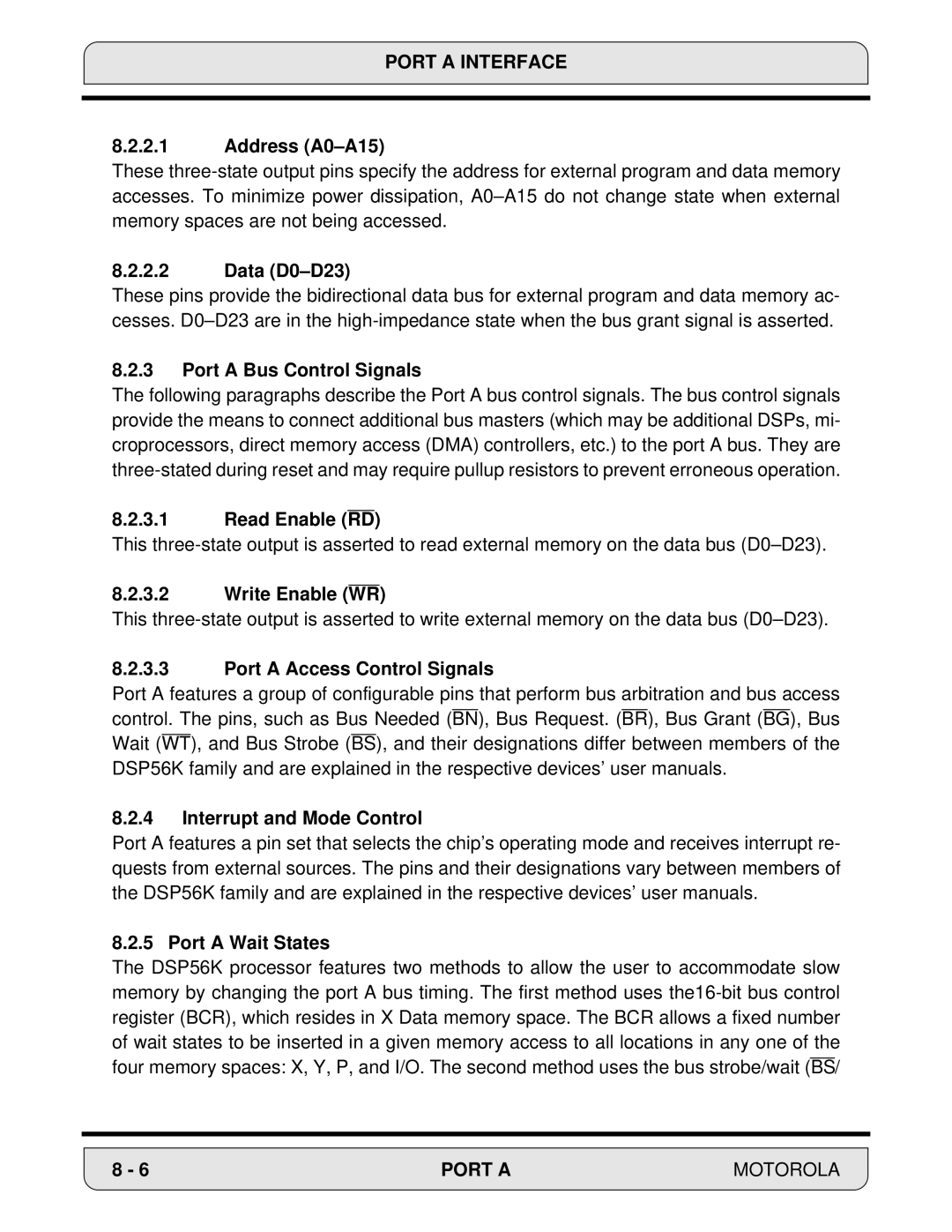
Port a Address and Data Bus Signals
Read/Write Control Signals
Program Memory Select PS
Data Memory Select DS
Read Enable RD
Port a Bus Control Signals
Write Enable WR
Address A0-A15
Port a Interface
Port a Interface Motorola
Motorola PLL Clock Oscillator
Section PLL Clock Oscillator
PLL Pins PLL Operation Considerations
PLL Clock Oscillator Introduction PLL Components
PLL Clock Oscillator Motorola
PLL Clock Oscillator Introduction
PLL Components
VCO
Area
Voltage Controlled Oscillator VCO
Low Power Divider LPD
Frequency Multiplier
PLL Control Register Pctl
Pctl Division Factor Bits DF0-DF3 Bits
Pctl Xtal Disable Bit Xtld Bit
Division Factor Bits DF0-DF3
Pctl Stop Processing State Bit Pstp Bit
Pctl PLL Enable Bit PEN Bit
Pctl Clock Output Disable Bits COD0-COD1 Bits
Pstp and PEN Relationship
Clock Output Disable Bits COD0-COD1
PLL Pins
Pctl Chip Clock Source Bit Csrc Bit
Pctl Ckout Clock Source Bit Ckos Bit
PLL Pins
Hardware Reset
PLL Operation Considerations
Operating Frequency
Operation with PLL Disabled
Changing the MF0-MF11 Bits
Change of DF0-DF3 Bits
Loss of Lock
Stop Processing State
Ckout Considerations
Synchronization Among EXTAL, CKOUT, and the Internal Clock
ON-CHIP Emulation OnCE
Section
Introduction
Debug Serial Input/Chip Status 0 DSI/OS0
ON-CHIP Emulation Introduction
24X24+56 →56-BIT MAC OnCE
OS1 OS0
Chip Status Information
Status
Debug Serial Output DSO
OnCE Command Register OCR
OnCE Controller and Serial Interface Debug Request Input DR
OnCE Controller and Serial Interface
OnCE Register Addressing
RS4 RS3 RS2 RS1 RS0
Go Command GO Bit
OnCE Controller and Serial Interface Exit Command EX Bit
Read/Write Command R/W Bit
Action
OnCE Status and Control Register Oscr
OnCE Decoder Odec
Memory Breakpoint Control BC0-BC3 Bits
MBO SWO TME BC3
Trace Mode Enable TME Bit
Memory Breakpoint Control Table
Reserved Bits 5-7
Trace Occurrence to Bit
Memory Breakpoint Occurrence MBO Bit
OnCE Memory Breakpoint Logic
Memory Address Latch Omal
Memory Lower Limit Register Omllr
Isbkpt
Memory High Address Comparator Omhc
OnCE Trace Logic
Memory Low Address Comparator Omlc
Memory Breakpoint Counter Ombc
Istrace
OnCE Trace Logic Block Diagram Trace Counter OTC
External Debug Request During Reset
Methods of Entering the Debug Mode
External Debug Request During Normal Activity
External Debug Request During Stop
Pipeline Information and Global Data BUS Register
Enabling Trace Mode
Software Request During Normal Activity
Enabling Memory Breakpoints
Pipeline Instruction Latch Register Opilr
Program Address BUS History Buffer
Global Data Bus Register Ogdbr
Read GDB Register
PAB Register for Decode Opabdr
PAB Register for Fetch Opabfr
OnCE Commands
Serial Protocol Description
PAB Fifo
Begin Debug Activity
Using the OnCE
Displaying a Specified Register
Motorola
Motorola
Motorola
Returning from Debug Mode to Normal Mode
Motorola
Motorola
Motorola
Motorola Additional Support
Section Additional Support
Motorola DSP News Motorola Field Application Engineers
User Support Motorola DSP Product Support
13 Reference Books and Manuals
Additional Support Motorola
Motorola Third Party Design
User Support
Prototyping
Verification
Motorola DSP Product Support
Macro Cross Assembler Features
11.2.4 DSP56KCCx Language Compiler Features
Simulator Features
DSP56KADSx Application Development System
11.4 Dr. BuB Electronic Bulletin Board
Audio
Dr. BuB Electronic Bulletin Board
Codec Routines
Dtmf Routines
Fast Fourier Transforms
Document ID Version Synopsis Size
Filters
Floating-Point Routines
Functions
Matrix Operations
Lattice Filters
=AB+Q
Reed-Solomon Encoder
Speech
Sorting Routines
Standard I/O Equates
Tools and Utilities
Following is a list of current DSP56200 related software
Motorola DSP News
Motorola Field Application Engineers
THIRD-PARTY Support Information 512
Training Courses 602 897-3665 or 800
Reference Books and Manuals
General DSP
Digital Audio and Filters
Digital Audio Signal Processing AN Anthology
Adaptive Signal Processing
Digital Filters and Signal Processing
ART of Digital AUDIO,
Controls
Programming Language
Fundamentals of Interactive Computer Graphics
CGM and CGI
Geometric Modeling
GKS Theory and Practice
Numerical Methods
Motorola DSP Manuals
Pattern Recognition
Telecommunications
Motorolaola Routines
Section Contents
Third Party Support
Motorola DSP Product Support
Application Development Systems
Support Integrated Circuits
DSP Marketing Information 512
DSP Applications Help Line 512
DSP THIRD-PARTY Support Information 512
DSP University Support 512
12.13 Dr. BuB Electronic Bulletin Board
DSP Training Courses 602 897-3665 or 800
Benchmarks
Document ID Version Synopsis Size
Filters
Floating-Point Routines
Functions
Lattice Filters
Document ID Version
Current DSP56200 Related Software
Reference Books and Manuals
Digital Audio and Filters
Leland B. Jackson Higham, MA Kluwer Academic Publishers
Illumination and Color in Computer Generated Imagery
Motorola DSP LINKER/LIBRARIAN Reference Manual
Motorola DSP Simulator Reference Manual
Motorola DSP Assembler Reference Manual
Motorola DSP56100 Family Manual
Motorola DSP56156 USER’S Manual
Statistical Spectral ANALYSIS, a Nonprobabilistic Theory
Digital Communications
Motorola Instruction SET Details
Appendix a Instruction SET Details
Section A.9 Instruction Sequence Restrictions
Section A.10 Instruction Encoding
Instruction SET Details Motorola
Instruction Guide
Appendix a Introduction
Notation
Address ALU Registers Operands
OMR
Address Operands
Binary Operators
Unary Operators
Condition Code Register CCR Symbols
Mode Register MR Symbols
MSP
Other Symbols
Addressing Modes
D a P X Y L XY
Table A-2 DSP56K Addressing Modes
M a
Table A-3 DSP56K Addressing Mode Encoding
Addressing Mode Modifiers
Binary M0-M7 Hex M0-M7 Addressing Mode Arithmetic
Table A-4 Addressing Mode Modifier Summary
Condition Code Computation
Condition Code Computation
Scaling Mode Bit Computation
Scaling Mode Signed Integer Portion
Condition Code Computation
Following notes apply to Table A-5
Parallel Move Descriptions
Instruction Descriptions
Absolute Value
Operation Assembler Syntax
Condition Codes
ABS D
Instruction Format
Opcode
Instruction Fields
Example
Add Long with Carry
ADC S,D
Add
Instruction Fields J d
ADD S,D
Shift Left and Add Accumulators
Addl S,D
Shift Right and Add Accumulators
Addr S,D
Logical Operation Assembler Syntax
S,D
Logical
Immediate with Control Register
CCR OMR
Arithmetic Shift Accumulator Left
ASL D
Arithmetic Shift Accumulator Right
ASR D
Bit Test and Change
Not affected Set if bit tested is set. Cleared otherwise
CCR Condition Codes
For other destination operands
Effective Addressing Mode
M R R R
Memory SpaceS Bit Number bbbbb
Absolute Short Address aaaaaa Memory SpaceS Bit Number bbbbb
Short Address pppppp Memory SpaceS Bit Number bbbbb
D D D D
Destination Register
Bchg
Bit Test and Clear
Condition Codes
For other destination operands
Bclr #n,Xea Bclr #n,Yea
Bclr #n,Xaa Bclr #n,Yaa
Bclr #n,Xpp Bclr #n,Ypp
Bclr #n,D
Bclr
Bit Test and Set Operation Assembler Syntax
Bset
Bit Test and Set
For other destination operands
Bset #n,Xea Bset #n,Yea
0 0 1 0 1 A a 1 b b b b b
0 0 1 0 1 P p 1 b b b b b
Bit Test and Set Instruction Format
Bset
Bit Test
For destination operand a or B
Btst #n,Xea Btst #n,Yea
Btst #n,Xaa Btst #n,Yaa
Btst #n,Xpp Btst #n,Ypp
Btst #n,D
Always cleared Always set
Clear Accumulator
CLR D
Compare
Instruction Fields S1,S2 J d
Compare Magnitude
Cmpm S1, S2
Debug
Timing 4 oscillator clock cycles Memory 1 program word
Cc Mnemonic Condition
CC HS
CS LO
CMP Y0, B
Enter Debug Mode Conditionally DEBUGcc
Instruction Fields Mnemonic
CC HS CS LO
DEC D
Decrement by One
Instruction Fields
Divide Interation
DIV S,D
Description
DIV
#$FE,CCR
ABS a A,B
DIV X0,A
TFR A,B
ADD X0,A
Signed quotient and a 48-bit signed remainder
Set if overflow bit V is set
0 0 0 0 0 J d 0 0
Start Hardware Loop Operation Assembler Syntax
Start Hardware Loop
Andi MR
At LA-2, LA-1, and LA
ORI MR
At LA-1
Start Hardware Loop At LA
Jclr Reset Jset RTI JMP RTS
JSR Wait
Other Restrictions
END1
END2
Xea, expr
Absolute Short Address aaaaaa Memory SpaceS
Immediate Short Data hhhh i i i i i i i
OMR SSL
Source
Start Hardware Loop
Immediately before Enddo
End Current do Loop
Opcode Instruction Fields
Logical Exclusive or
EOR S,D
Illegal
Illegal Instruction Interrupt
None Timing 8 oscillator clock cycles Memory 1 program word
Increment by One
INC D
Jump Conditionally
Jcc
0 0 1 1 1 C C a a a a A a a a a a
Jcc ea
M R R R
Jump if Bit Clear
For other source operands Condition codes are not affected
Jclr #n,Xea,xxxx Jclr #n,Yea,xxxx
Jclr #n,Xaa,xxxx Jclr #n,Yaa,xxxx
Jclr #n,Xpp,xxxx Jclr #n,Ypp,xxxx
Source Register
Jump
0 0 1 0 1 M M R R R 0 0 0 0 0
Jump to Subroutine Conditionally
Example
Instruction Format
Effective Addressing Mode M M M R R R Mnemonic C C C C
Jsclr
Jump to Subroutine if Bit Clear
Condition Codes
Jsclr #n,Xea,xxxx Jsclr #n,Yea,xxxx
Jsclr #n,Xaa,xxxx Jsclr #n,Yaa,xxxx
Short Address aaaaaa Memory SpaceS Bit Number bbbbb
Jsclr #n,S,xxxx
Jsclr
Jump if Bit Set Operation Assembler Syntax
Jset
Jump if Bit Set
Jset #n,Xea,xxxx Jset #n,Yea,xxxx
Jump if Bit Set Instruction Format
Jset #n,Xpp,xxxx Jset #n,Ypp,xxxx
Jset #n,S,xxxx
Jump to Subroutine
JSR
Jump to Subroutine if Bit Set
Example
Jsset #n,Xea,xxxx Jsset #n,Yea,xxxx
Jsset #n,Xaa,xxxx Jsset #n,Yaa,xxxx
Jsset #n,Xpp,xxxx Jsset #n,Ypp,xxxx
Jsset #n,S,xxxx
Logical Shift Left
LSL D
Logical Shift Right
LSR D
Load Updated Address
Dest. Addr. Reg. D
PLY Mode
Signed Multiply-Accumulate
MAC X0,X0,A
Instruction Fields S1∗S2 Sign
Instruction Fields Sign
Sssss Constant
Signed Multiply-Accumulate and Round
Signed Multiply-Accumulate and Round Macr
Macr -Y0 #10, B
±S,#n,D
Move S,D
Move Data
Condition Codes
Move
Move
No Parallel Data Move Operation Assembler Syntax
No Parallel Data Move Instruction Format Opcode
Tinations are not allowed within the same instruction
Immediate Short Data Move
ABS B #$18,R1 Take absolute value of B, #$18R1
#xx=8-bit Immediate Short Data=iiiiiiii
Sign Ext Zero
Register to Register Data Move
MACR-X0,Y0,A
Instruction Format Opcode
Instruction Fields Or D Sign Ext Zero
Address Register Update Operation Assembler Syntax
R R R
Address Register Update
Memory Data Move Operation Assembler Syntax
Memory Data Move Example
Effective Register W Addressing Mode
Memory Data Move Instruction Format
M R R
Memory Data Move Sign Ext Zero
Register W Absolute Short Address a a a a a a
Instruction Descriptions
Xea D1 S2 D2 Xea,D1
Class I Example
Memory and Register Data Move
Memory and Register Data Move Class II Example
Memory and Register Data Move Condition Codes
Class I Instruction Format
R R
Memory and Register Data Move S1,D1 Sign Ext Zero
Sign Ext Zero Move Opcode
Memory and Register Data Move Class II Instruction Format
Memory Data Move Operation Assembler Syntax
After Execution $00123456000000
Yea,D #xxxxxx,D
Memory Data Move Sign Ext Zero
Register W Absolute Short Address aaaaaa
Instruction Descriptions
Class
Register and Y Memory Data Move
Addl B,A B,X1 YR6-N6,B 2∗A+B A, update X1,B and R6
By R1 and postincrement R1 Move Y0 to B
Register and Y Memory Data Move Class II Example
S1,D1 Yea,D2 . . . . . S1,D1 S2,Yea S1,D1 #xxxxxx,D2
S1 d Sign Ext Zero S2,D2
Register and Y Memory Data Move Instruction Fields
Dest
Register and Y Memory Data Move Class II Instruction Format
Long Memory Data Move Operation Assembler Syntax
CMP Y0,B
Long Memory Data Move
Long Memory Data Move Instruction Format
0 0 L 0 L A a a
XY Memory Data Move Operation Assembler Syntax
Mpyr X1,Y0,A
XY Memory Data Move Example
XY Memory Data Move Instruction Format
XY Memory Data Move Effective Register
Sign Ext Zero Addressing Mode R r
Move Control Register
Movec
Movec LC,X0 move LC into
2316 158 0 0 0 1 0 1 W 1 M M M R R R 0 s 1 d d d d d
Memory Space s S1, D1 D d d
Movec Xaa,D1 Movec S1,Xaa Movec Yaa,D1 Movec S1,Yaa
Instruction Fields Register S1, D1 D d d
Movec S1,D2 Movec S2,D1
Memory Space s
S2, D2 e e e e e e Sign Ext Zero
#xx=8-bit Immediate Short Data=i i i i i i i
Move Program Memory
Movem
Movem PR5+N5, LC
Movem S,Pea Movem Pea,D
D d d d Sign Ext Zero
Movem S,Paa Movem Paa,D
Movep
Movep
$FFFE BCR
Move Peripheral Data
Instruction Format X or Y Reference
Effective Memory Space Addressing Mode
Peripheral Space
Peripheral
Instruction Format P Reference
Effective Peripheral Space S Addressing Mode
Peripheral Space S Peripheral W
Instruction Format Register Reference
Signed Multiply Operation
MPY MPY
Signed Multiply
Signed Multiply Instruction Fields S1∗S2
Instruction Fields Sign Sssss constant
Signed Multiply Instruction Format
Signed Multiply and Round
Instruction SET Descriptions
Instruction Fields S1∗S2 Q Q Q Sign k
Mpyr ±S,#n,D
Negate Accumulator
NEG D
PC+1PC NOP
No Operation
None Timing 2 oscillator clock cycles Memory 1 program word
Norm R3,A
Normalize Accumulator Iteration
Normalize Accumulator Iteration Norm
Logical Complement
Not D
Logical Inclusive or Operation Assembler Syntax
Logical Inclusive or
Or Immediate with Control Register
Condition codes are not affected using these operands
Repeat Next Instruction
Temp LC
Temp LC LC Temp S LC REP
Jclr RTI JMP RTS Jset Stop
Immediately after REP
Jsclr Wait JSR Enddo
REP MAC X1,Y1,A
Condition Codes
REP Xea REP Yea
Absolute Short Address aaaaaa Memory Space s
Immediate Short Data hhhh i i i i i i i i
Instruction Fields D d d d
REP S
Dition Code Computation
Reset On-Chip Peripheral Devices
None Timing 4 oscillator clock cycles Memory 1 program word
Round Accumulator
RND a #$123456,X1 B,Y1
Condition Codes
RND D
Rotate Left
Opcode
Rotate Right
ROR D
Return from Interrupt
Opcode Instruction Fields
Return from Subroutine
Opcode
Subtract Long with Carry
SBC
Condition Codes
SBC S,D
Stop Instruction Processing
Restrictions
Subtract
SUB S,D
Shift Left and Subtract Accumulators
Subl S,D
Shift Left and Subtract Accumulators Subl Condition Codes
Shift Right and Subtract Accumulators
Subr S,D
Shift Right and Subtract Accumulators Subr Condition Codes
Software Interrupt
Operation Assembler Syntax Begin SWI exception processing
SWI
Opcode Instruction Fields
Cc’’ Mnemonic Condition
Transfer Conditionally
CMP X0,A
C C
S1,D1 Mnemonic
J D
Transfer Data ALU Register
TFR S,D
Test Accumulator
TST S
Wait for Interrupt
Condition Codes
Motorola Benchmark Programs
Appendix B Benchmark Programs
Benchmark Programs Motorola
Section B.1 Introduction Section B.2 Benchmark Programs
Introduction
Cycles
Table B-1 27-MHz Benchmark Results for the DSP56001R27
Benchmark Programs Motorola
Figure B-1 20-Tap FIR Filter Example Sheet 1
Benchmark Programs Motorola
Figure B-1 20-Tap FIR Filter Example Sheet 2
Benchmark Programs Motorola
Figure B-2 Radix 2, In-Place, Decimation-In-Time FFT Sheet 1
Benchmark Programs Motorola
Benchmark Programs
Motorola Benchmark Programs
+ yn 1wn-1 Ai1 bi1
Benchmark Programs
Benchmark Programs
Benchmark Programs
$FFC0
Figure B-5
Benchmark Programs
Benchmark Programs
Benchmark Programs
Benchmark Programs
Benchmark Programs
128 3846 256 8656 512 19296
Benchmark Programs
DSP56100 Family Manual Trouble Report
DSP56100 Family Manual Trouble Report
Index
Index
Index
Index
Index
AGU -6 data ALU -19 program control unit -8 summary -17 Pvcc
Zero Bit -10, A-17